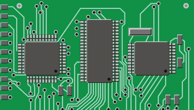
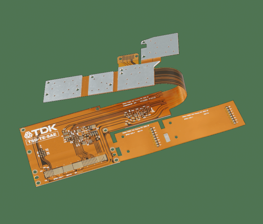
PCB Design Best Practices for High-Speed Circuits
-
1. Vertical Wiring Principle
When wiring between adjacent layers in a PCB, it is crucial to follow the vertical wiring principle. Failure to do so may result in crosstalk between lines and increased EMI radiation. Therefore, it is recommended to align wiring in both horizontal and vertical directions to mitigate crosstalk effectively.
-
2. Topological Structure in High-Speed PCB Design
Controlling the characteristic impedance of the circuit board and designing the topological structure play a vital role in the success of high-speed PCB designs, especially under multi-load conditions. While a daisy-chain topology is suitable for lower frequencies, a star-shaped symmetrical structure is preferred for high-speed designs.
-
3. Resonance Rule for Trace Length
Resonance can occur when the length of a signal trace aligns with a quarter of the signal wavelength, leading to electromagnetic interference. It is essential to verify the trace length and frequency to prevent resonance-related issues.
-
4. Return Path Guidelines
High-speed signals, such as clocks, require a reliable return path to minimize radiation. Keeping the return path as short as possible reduces the area enclosed by the signal and return paths, thereby decreasing radiation levels.
-
5. Decoupling Capacitor Placement
Proper placement of decoupling capacitors near power supply pins is critical for their effectiveness. Placing decoupling capacitors incorrectly can compromise their decoupling function. It is essential to minimize the area enclosed by power traces and ground connections of the capacitor for optimal performance.


 العربية
 简体中文
简体中文 Nederlands
 English
 Français
 Deutsch
 Italiano
 日本語
日本語 한국어
한국어 Português
 Русский
 Español
 ไทย
ไทย