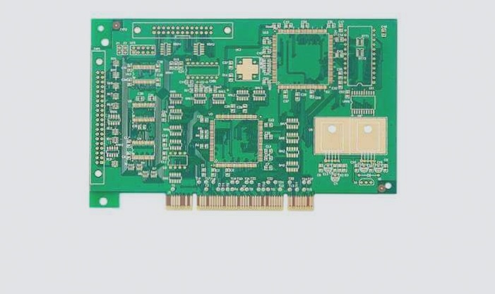
Enhancing Dynamic Range with Modern IC Amplifiers on PCBs
Modern IC amplifiers with low harmonic distortion are crucial for improving dynamic range in various applications. However, improper PCB layout can lead to a degradation in distortion performance by up to 20 dB.
High-Speed Amplifier Configuration
- Utilize two sets of bypass capacitors for high-speed amplifiers.
- One set with larger capacitance (1 µF to 10 µF), the other with smaller capacitance (1 nF to 100 nF).
- Proper bypassing requires multiple capacitor sets to prevent self-resonance and ensure low-impedance ground paths.
Decoupling and Termination
High-quality chip capacitors with low inductance are ideal for decoupling in amplifier circuits. The resistor RT terminates the amplifier’s input to match source impedance with measurement instruments.
Current Path and Grounding
Amplifiers must provide or sink current for loads. High-frequency current flows through bypass capacitors, forming loops for effective current return paths.
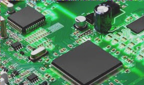
PCB Layout Considerations
- Proper layout analysis helps reduce second harmonic distortions in amplifier circuits.
- Optimal layouts minimize inductance by placing bypass capacitors close to power supplies and load grounds.
Improving Distortion Index
Enhanced PCB layouts can boost the second harmonic distortion index by 3dBc to 18dBc across different frequencies, offering more effective performance.
Differential Bypassing
Implementing differential bypassing with two sets of capacitors can help avoid grounding issues and improve overall amplifier performance.
Optimizing PCB Layout for Improved Performance
Optimizing the layout of a PCB can have a significant impact on its performance. One crucial aspect is ensuring proper grounding of the load and bypass capacitors to minimize inductance and reduce error voltage caused by high-frequency ground current.
By integrating high-frequency current before it returns to the load, issues like half-wave rectification and odd harmonic components can be minimized, resulting in lower distortion in the current channel.
When dealing with poor bypassing in a PCB layout, keeping the bypass capacitor trace short and minimizing the use of vias is essential. If vias are necessary, utilizing two parallel vias can reduce inductance, and increasing the diameter of through holes can further decrease it.
For layouts where the feedback network needs grounding and the closed-loop gain exceeds one, optimizing the grounding method of the feedback network is crucial. This ensures that the high-frequency current flowing through the feedback network returns to the power supply via the bypass capacitor, effectively minimizing inductance increase.