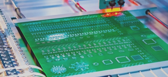
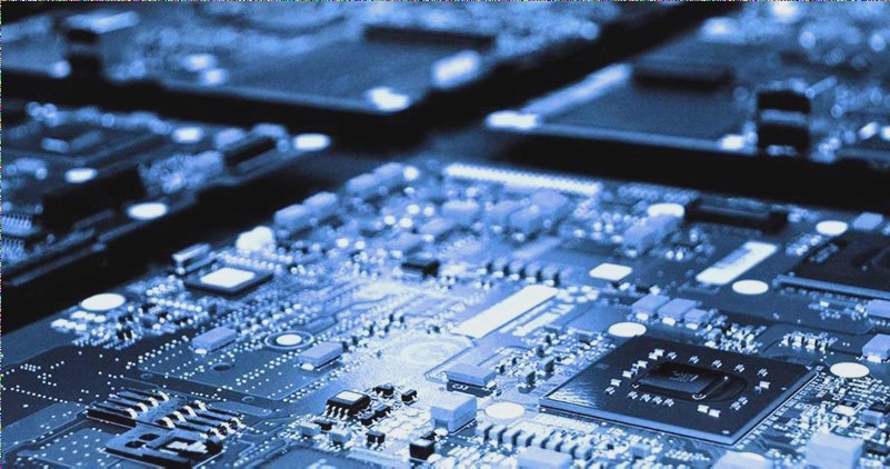
Reasonable layout of components in PCB design. By paying attention to the trend of environmental informationization and the development of various environmental protection technologies, PCB factories can leverage big data to monitor pollution and governance outcomes, allowing for timely identification and resolution of environmental issues. Adapting to the production concepts of the new era, these factories should continuously enhance resource utilization to achieve green production. The goal is to enable the PCB industry to adopt an efficient, economical, and environmentally friendly production model, actively responding to national environmental protection policies.
1. Aesthetic considerations should not only include the neat and orderly arrangement of components but also the elegance and smoothness of the wiring. Laypersons often focus more on the former to evaluate circuit design, prioritizing aesthetics when performance requirements are lenient. However, in high-performance applications where double-sided boards are encapsulated and typically hidden, the aesthetics of wiring should take precedence.
2. Stressed circuit boards must withstand various external forces and vibrations during installation and operation. Therefore, the board should have a rational shape, and the positioning of all holes (screw holes, special-shaped holes) must be well-planned. Typically, the distance from the hole to the board’s edge should exceed the hole’s diameter. Additionally, the weakest section of the board, created by special-shaped holes, should maintain adequate bending strength. Connectors extending directly from the device housing must be securely fixed to ensure long-term reliability.
—
Let me know if you need any further adjustments!

3. Heated: For high-power, high-heat devices, it is crucial to ensure effective heat dissipation and to position them appropriately. In sophisticated analog systems, special attention must be given to the impact of the temperature field generated by these devices on sensitive preamplifier circuits. Generally, high-power components should be designed as separate modules, incorporating thermal isolation measures between them and the signal processing circuit.
4. Signal interference is the primary concern in PCB layout design. Key considerations include: separating or isolating weak signal circuits from strong signal circuits; keeping AC circuits distinct from DC circuits; segregating high-frequency components from low-frequency ones; paying attention to signal line orientation; optimizing ground line layout; and implementing effective shielding and filtering. These principles have been extensively discussed in literature, so I will not reiterate them here.
5. Installation pertains to the specific application context, ensuring that the circuit board is smoothly integrated into the chassis, casing, or slot, while avoiding space interference, short circuits, and other issues. It is essential for designated connectors to align correctly with their corresponding positions on the chassis or casing. In light of the increasing emphasis on environmental informationization and advancements in various environmental protection technologies, PCB manufacturers should leverage big data to monitor pollution and governance outcomes, allowing for timely identification and resolution of environmental issues. By aligning with modern production concepts, companies can enhance resource utilization and achieve green production. The PCB industry should strive for an efficient, cost-effective, and environmentally friendly production model, actively supporting national environmental protection policies.


