Understanding PCB Copper Thickness, Line Width, and Current
Before delving into the relationship between PCB board design copper thickness, line width, and current, it’s essential to grasp the conversion between ounces, inches, and millimeters of PCB copper thickness.
Conversion Relationship:
- 1 ounce = 0.0014 inches = 0.0356 mm
- 2 ounces = 0.0028 inches = 0.0712 mm
Empirical Formulas:
The relationship between PCB design line width (W) and copper thickness (T) can be expressed as: W = 0.15 * T.
Factors Affecting Current-Carrying Capacity:
The current-carrying capacity is influenced by wire impedance (0.0005 * (L/W)), number of components, pads, and vias on the line.
Additional Considerations:
Factors like pads and vias affect the current-carrying capacity of traces. Soldering on component legs can increase current capacity between pads. To prevent trace burnout, increasing trace width or adding a solder layer post-soldering can be effective.
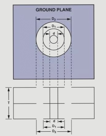
Enhancing Current Distribution:
Improving current distribution between traces and pads is crucial in high-current boards. Methods illustrated in the diagram below help disperse current uniformly, reducing the risk of circuit burnout.
The Importance of Copper Thickness and Trace Width in PCB Design
When designing PCBs, understanding the relationship between copper foil thickness, trace width, and current is crucial for signal integrity and overall performance. Here are some key points to consider:
1. Reference Data Table for Current Carrying Values
- For designs with lower currents, it’s recommended to add a 10% margin to table values to ensure compliance.
- For single-layer designs with 35 µm copper thickness, a 1:1 ratio (1 mm trace can carry 1 A) is suitable for currents up to 105°C.
2. Derating Trace Widths for High Current Applications
- When dealing with significant currents, trace widths should be derated by 50% from table values for cautious selection.
- Understanding the “OZ” unit for copper thickness (1 OZ = 35µm) is essential in PCB design.
3. Line Width Determination for High Current Paths
Correlating copper thickness with current requirements aids in selecting appropriate line widths.
4. Utilizing Impedance Calculation Software
PCB board temperature impedance calculation software helps determine parameters like line width, current capacity, and impedance, streamlining capacity calculations based on specified conditions.
5. Estimating Allowable Currents with Empirical Formulas
The formula I=KT^0.44A^0.75 assists in estimating safe currents, optimizing trace design for secure current handling.
6. Importance of Line Widths and Copper Deposition
Choosing the right line width and copper thickness is crucial to prevent overheating and damage during high current surges, ensuring board integrity.
Understanding the nuances between different copper deposition methods is essential for thermal dissipation and overcurrent capabilities, impacting overall PCB performance and reliability.