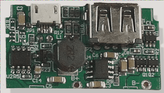
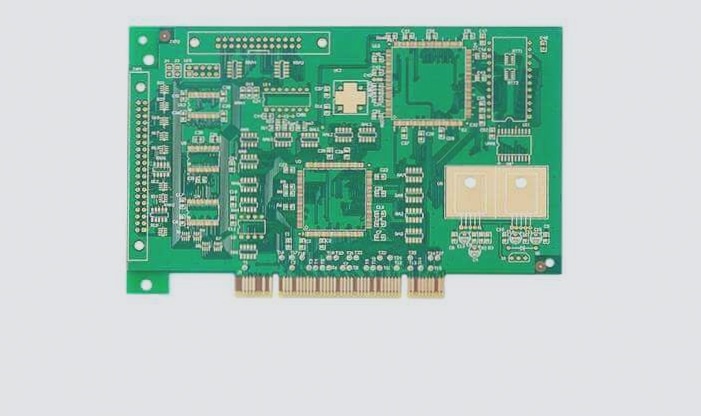
In the design of PCB boards, the PCB’s anti-ESD capabilities can be achieved through layering, appropriate layout, and installation. During the design process, most modifications involve adding or reducing components based on predictions. By adjusting the PCB layout and routing, effective ESD prevention can be achieved. The following outlines some common precautions:
1. Use multilayer PCBs whenever possible:
Compared to double-sided PCBs, multilayer PCBs with ground and power planes, and closely spaced signal line-ground spacing, can significantly reduce common mode impedance and inductive coupling. This reduction can be as much as 1/10 to 1/100 of that seen in double-sided PCBs. It is advisable to place each signal layer as close as possible to a power or ground layer. For high-density PCBs that feature components on both top and bottom surfaces, short connection lines, and numerous fills, consider utilizing inner layer traces.
2. For double-sided PCBs, employ tightly interlaced power and ground grids:
Ensure that power lines run adjacent to ground lines, maximizing connections between vertical and horizontal lines or filled areas. The grid size on one side should ideally be ≤ 60mm, with a preference for sizes ≤ 13mm if feasible.

3. Ensure that each circuit is as compact as possible.
4. Place all connectors as far apart as feasible.
5. Maintain a consistent “isolation zone” between the chassis ground and circuit ground on every layer; aim for a separation distance of 0.64mm where feasible.
6. During PCB assembly, refrain from soldering on the top or bottom pads. Use screws with integrated washers to ensure close contact between the PCB and the metal chassis/shielding layer or supporting ground plane.
7. If feasible, introduce power cords from the center of the board, avoiding areas directly susceptible to ESD.
8. Below connectors leading outside the chassis (prone to ESD), place extensive chassis ground or polygonal fillings on all PCB layers, connecting them with vias approximately every 13mm.
9. Position mounting holes along the board edge, connecting top and bottom pads directly to chassis ground without solder resist around these holes.
10. Near mounting holes on the top and bottom layers, connect chassis ground and circuit ground with 1.27mm-wide traces every 100mm along the chassis ground trace. Adjacent to these connections, place pads or mounting holes for potential jumpers with magnetic beads or high-frequency capacitors to maintain circuit openness.
11. If the PCB will not be housed in a metal chassis or shielding, avoid applying solder resist to top and bottom chassis ground traces to enable them as ESD discharge paths.
12. Implement a ring ground around the circuit as follows:
(1) Surround the entire perimeter, excluding edge connectors and chassis ground, with a circular ground path.
(2) Ensure the ring ground width exceeds 2.5mm across all layers.
(3) Connect via holes in a ring pattern spaced approximately 13mm apart.
(4) Tie the ring ground to the multilayer circuit’s common ground.
(5) For double-sided PCBs in metal cases, connect the ring ground to the circuit’s common ground. For unshielded PCBs, connect it to the chassis ground. Maintain a 0.5mm gap at least once in the ring ground (across all layers) to prevent large loops. Ensure a minimum 0.5mm separation between signal traces and the ring ground.
13. In ESD-vulnerable areas, place a ground wire near each signal line.
14. Position I/O circuits in close proximity to corresponding connectors.
15. Locate ESD-sensitive circuits toward the center of the PCB to benefit from shielding effects provided by surrounding circuits.
16. Install transient protectors at reception ends, using short and thick wires (preferably less than 3 times the width in length) to connect to chassis ground. Directly connect signal and ground wires from the connector to the transient protector before extending to other circuitry.
17. Typically, place series resistors and magnetic beads at reception ends. For ESD-prone drivers, consider adding series resistors or magnetic beads at the driving end.
18. Place a filter capacitor at the connector or within 25mm of the reception circuit.
19. Use short and thick wires to connect capacitors to chassis ground or reception circuit ground (length less than 3 times the width).
20. Keep PCB signal lines as short as possible.
21. Parallel a ground wire if signal wire length exceeds 300mm.
22. Minimize loop area between PCB signal lines and corresponding loops. Alternate positions of signal lines and ground lines every few centimeters for long signal lines. Route drive signals from the network center to multiple receiving PCB circuits if feasible.
23. Fill unused areas with copper and connect filling grounds across all layers at intervals of 60mm.
1. Use multilayer PCBs whenever possible:
Compared to double-sided PCBs, multilayer PCBs with ground and power planes, and closely spaced signal line-ground spacing, can significantly reduce common mode impedance and inductive coupling. This reduction can be as much as 1/10 to 1/100 of that seen in double-sided PCBs. It is advisable to place each signal layer as close as possible to a power or ground layer. For high-density PCBs that feature components on both top and bottom surfaces, short connection lines, and numerous fills, consider utilizing inner layer traces.
2. For double-sided PCBs, employ tightly interlaced power and ground grids:
Ensure that power lines run adjacent to ground lines, maximizing connections between vertical and horizontal lines or filled areas. The grid size on one side should ideally be ≤ 60mm, with a preference for sizes ≤ 13mm if feasible.

3. Ensure that each circuit is as compact as possible.
4. Place all connectors as far apart as feasible.
5. Maintain a consistent “isolation zone” between the chassis ground and circuit ground on every layer; aim for a separation distance of 0.64mm where feasible.
6. During PCB assembly, refrain from soldering on the top or bottom pads. Use screws with integrated washers to ensure close contact between the PCB and the metal chassis/shielding layer or supporting ground plane.
7. If feasible, introduce power cords from the center of the board, avoiding areas directly susceptible to ESD.
8. Below connectors leading outside the chassis (prone to ESD), place extensive chassis ground or polygonal fillings on all PCB layers, connecting them with vias approximately every 13mm.
9. Position mounting holes along the board edge, connecting top and bottom pads directly to chassis ground without solder resist around these holes.
10. Near mounting holes on the top and bottom layers, connect chassis ground and circuit ground with 1.27mm-wide traces every 100mm along the chassis ground trace. Adjacent to these connections, place pads or mounting holes for potential jumpers with magnetic beads or high-frequency capacitors to maintain circuit openness.
11. If the PCB will not be housed in a metal chassis or shielding, avoid applying solder resist to top and bottom chassis ground traces to enable them as ESD discharge paths.
12. Implement a ring ground around the circuit as follows:
(1) Surround the entire perimeter, excluding edge connectors and chassis ground, with a circular ground path.
(2) Ensure the ring ground width exceeds 2.5mm across all layers.
(3) Connect via holes in a ring pattern spaced approximately 13mm apart.
(4) Tie the ring ground to the multilayer circuit’s common ground.
(5) For double-sided PCBs in metal cases, connect the ring ground to the circuit’s common ground. For unshielded PCBs, connect it to the chassis ground. Maintain a 0.5mm gap at least once in the ring ground (across all layers) to prevent large loops. Ensure a minimum 0.5mm separation between signal traces and the ring ground.
13. In ESD-vulnerable areas, place a ground wire near each signal line.
14. Position I/O circuits in close proximity to corresponding connectors.
15. Locate ESD-sensitive circuits toward the center of the PCB to benefit from shielding effects provided by surrounding circuits.
16. Install transient protectors at reception ends, using short and thick wires (preferably less than 3 times the width in length) to connect to chassis ground. Directly connect signal and ground wires from the connector to the transient protector before extending to other circuitry.
17. Typically, place series resistors and magnetic beads at reception ends. For ESD-prone drivers, consider adding series resistors or magnetic beads at the driving end.
18. Place a filter capacitor at the connector or within 25mm of the reception circuit.
19. Use short and thick wires to connect capacitors to chassis ground or reception circuit ground (length less than 3 times the width).
20. Keep PCB signal lines as short as possible.
21. Parallel a ground wire if signal wire length exceeds 300mm.
22. Minimize loop area between PCB signal lines and corresponding loops. Alternate positions of signal lines and ground lines every few centimeters for long signal lines. Route drive signals from the network center to multiple receiving PCB circuits if feasible.
23. Fill unused areas with copper and connect filling grounds across all layers at intervals of 60mm.


