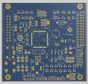
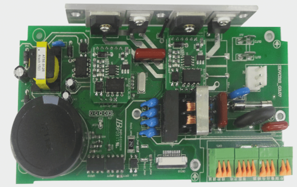
PCB, also known as Printed Circuit Boards, facilitate circuit connections and enable the functioning of electronic components. They are crucial components in the design of power circuits. This article will introduce the fundamental rules of PCB layout and wiring.

1. Basic Rules of Component Layout
1. Arrange components according to circuit modules, where related circuits performing the same function constitute a module. Components within a module should be placed close together for optimal concentration, while ensuring digital and analog circuits remain separate.
2. Maintain a minimum distance of 1.27mm around non-mounting holes such as positioning and standard holes; avoid placing components within 3.5mm (for M2.5) and 4mm (for M3) of mounting holes such as screws.
3. Ensure vias are not positioned beneath components like horizontally mounted resistors, inductors (through-hole), and electrolytic capacitors to prevent potential short circuits after wave soldering.
4. Maintain a 5mm distance between the outer edge of components and the board edge.
5. Ensure a minimum 2mm gap between the outer pad of a mounted component and adjacent components.
6. Metal shell components and parts (such as shielding boxes) must not contact other components or come close to printed lines and pads; maintain a spacing greater than 2mm. Positioning, fastener installation, elliptical, and square holes on the board should be at least 3mm away from the board edge.
7. Heating elements should be distanced from wires and thermal elements; distribute high-heat elements evenly across the board.
8. Place power sockets around the board periphery, ensuring bus bar terminals connected to these sockets are on the same side. Avoid positioning power sockets and soldered connectors between other connectors to facilitate their soldering and cable tying.
9. Arrange IC components on one side, clearly marking polar components. Ensure polarity markings on the same board do not exceed two directions; if two directions are necessary, they should be perpendicular.
10. Maintain appropriate wiring density on the board; areas with significant density differences should be filled with copper mesh greater than 8mil (0.2mm).
11. Avoid through-holes on pad areas to prevent solder paste loss during component soldering. Critical signal lines should not pass between socket pins.
12. Ensure unilateral alignment of surface-mount components, with consistent character and packaging orientations.
13. For polar devices, ensure consistent polarity marking directions on the board.
2. Component Wiring Rules
1. Prohibit wiring within 1mm of the PCB edge and within 1mm around mounting holes in areas where the wiring area is ≤1mm.
2. Power lines should be adequately wide, not less than 18mil; signal line width should not be less than 12mil. CPU input and output lines should not be less than 10mil (or 8mil), with line spacing not less than 10mil.
3. Standard via hole size should not be less than 30mil.
4. For components such as dual in-line packages: pad size should be 60mil with a 40mil aperture; for 0805 surface mount, pad size should be 55mil with a 42mil aperture. Electrolytic capacitors should have a 51x55mil (0805 surface mount) pad size with a 28mil aperture for direct plugging.
5. Ensure power and ground wires are radially arranged as much as possible; signal lines must not create loops.
2.1 Anti-Electromagnetic Interference Measures
1. Systems with high microcontroller clock frequencies and fast bus cycles require special attention.
2. Systems containing high-power, high-current drive circuits (e.g., spark-generating relays) and weak analog signal circuits with high-precision A/D conversion circuits necessitate careful consideration.
2.2 Methods to Enhance Anti-Electromagnetic Interference Capability
1. Select microcontrollers with lower external clock frequencies to reduce noise and enhance system interference resistance.
2. Address signal transmission distortion issues by considering signal reflection and impedance matching, particularly for high-speed CMOS circuits.
3. Minimize interference between signal lines by optimizing layout and using shielding techniques.
4. Mitigate power supply noise by careful routing and design considerations.
5. Consider high-frequency characteristics of PCBs and components, addressing distributed parameters that impact signal integrity and noise emission.
6. Partition component layout to segregate analog signals, high-speed digital circuits, and noise sources effectively.
This revision aims to streamline and clarify guidelines for PCB component layout and wiring, emphasizing best practices for minimizing interference and ensuring signal integrity.


