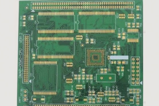
When addressing the core principles of high-speed PCB design, it’s essential to focus on the following key aspects:
### 1. Power Circuit Design
The power supply is the backbone of stable operation for any electronic device. While power supply design challenges may not always be the most technically demanding, any issues with operational stability are often rooted in power-related problems.
The primary focus of power supply design lies in optimizing the functional design of the power module, enhancing conversion efficiency, and ensuring the integrity of power channels. These designs must adhere to strict technical specifications and industry standards. For applications involving sensitive power supplies or those with high current demands, Power Integrity (PI) simulation becomes crucial. This helps address challenges like voltage drop, dynamic impedance, and noise, ensuring that the power supply remains stable under varying operational conditions.

### High-Speed Signal Design in PCB: Challenges and Solutions
#### 1. High-Speed Parallel Signal Design
High-speed parallel signal designs, including DDR3, DDR4, and similar circuits, are crucial in high-performance electronics. This is especially true in Memory Down (onboard memory) designs, where specific care must be taken. While adhering strictly to the original layout guidelines is essential, it is equally important to optimize the design through simulation analysis to ensure signal integrity.
In most parallel signal designs, controlling both absolute and relative signal lengths is key. Designers must follow the corresponding chip specifications to achieve the desired performance. Additionally, managing via count, signal trace length distribution, and crosstalk mitigation will satisfy most design requirements. These factors are critical for ensuring stable high-speed signal performance.
#### 2. High-Speed Serial Signal Design
In recent years, high-speed serial signals have become more prominent as traditional parallel bus interfaces, such as IDE, have been replaced by serial connections like SATA. High-speed serial signal applications are growing rapidly across various industries.
The most common high-speed serial channels today include PCIE, SATA, SAS, LVDS, USB 3.0, and high-speed optical networks. These channels have seen speed increases to 5G, 8G, 10G, 28G, and even 56Gbps. As signal speeds increase, it is essential to follow the design guidelines specific to high-speed signaling. Neglecting these rules can lead to significant signal integrity issues, including data loss and signal distortion. Proper analysis and optimization of signal integrity are necessary to ensure reliable performance.
#### 3. Key Technical Areas in High-Speed PCB Design
In addition to parallel and serial signal designs, several other technical considerations play a vital role in high-speed PCB design. These include analog signal design, RF signal management, digital-analog mixed signal design, and manufacturability (DFM) and design for excellence (DFX) considerations. Furthermore, EMC (electromagnetic compatibility) must be prioritized to ensure compliance with industry standards and avoid interference issues.
Each of these areas comes with its own set of specific rules and requirements. For those looking to deepen their understanding, exploring each of these fields is highly recommended.
#### 4. The Complexity of High-Speed PCB Design
High-speed PCB design is a multifaceted and complex process that cannot be fully explained in just a few words. Every professional field has its own set of methodologies, processes, and rules. This makes high-speed PCB design a highly technical and systems-oriented challenge, requiring years of experience and continuous learning. Even within the same industry, different subfields may have vastly different design rules and methodologies.
As the saying goes, “interlacing is like a mountain.” Transitioning from one subfield to another—even within the same industry—can result in limited transferability of skills and knowledge. For instance, moving from low-end consumer product design to military or communication product design could require a complete reevaluation of design approaches due to differing rules and knowledge systems. This illustrates the importance of not just selecting a PCB industry but also understanding the nuances of specific subfields.
#### 5. Solving High-Speed PCB Design Challenges from Multiple Perspectives
To tackle the technical challenges of high-speed PCB design, it’s necessary to approach them from multiple angles. Below is a summary of the core solutions for overcoming these challenges:
– **Signal Integrity (SI) Analysis**: Analyzing signal integrity to guide and optimize the PCB design process. This step ensures minimal signal degradation and improves overall performance.
– **Power Integrity (PI) Analysis**: Improving the power supply network design and optimizing decoupling capacitor placement to maintain stable power delivery to the components.
– **Design for Manufacturability (DFM)**: Optimizing the PCB design for efficient manufacturing, which reduces production costs and enhances product quality.
– **Design for Assembly (DFA)**: Analyzing the design for easier assembly, maintenance, and testing, ultimately improving production efficiency and reducing errors.
– **Electromagnetic Compatibility (EMC) Analysis**: Focusing on optimizing the electromagnetic interference (EMI) and electrostatic discharge (ESD) characteristics to meet regulatory requirements and prevent signal interference.
– **Other Considerations**: Factors like cost optimization, structural heat dissipation, long-term reliability, and product lifecycle must also be taken into account to ensure a balanced design approach.
By addressing these challenges from a comprehensive and systematic perspective, PCB designers can create high-performance, reliable, and cost-effective solutions that meet the demands of modern high-speed electronics.