1. **Optimizing Surface Mount and Crimping Components**
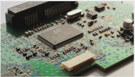
Surface mount components and crimping components are highly manufacturable. With advancements in component packaging technology, most components are now available in formats suitable for reflow soldering, including through-hole components that can be soldered using this method. Achieving complete surface assembly in design can significantly enhance both the efficiency and quality of the assembly process. Crimping components, primarily multi-pin connectors, also boast excellent manufacturability and connection reliability, making them a preferred choice.
2. **Focusing on the PCBA Assembly Surface: Considering Package Size and Pin Spacing as a Whole**

1. The most significant influence on overall board manufacturability stems from package size and pin spacing. When selecting surface mount components, it is essential to choose packages with similar process capabilities or those compatible with solder paste printing on a stencil of a specific thickness for a given PCB size and assembly density. For instance, mobile phone boards typically use packages suitable for solder paste printing with a 0.1mm thick stencil.
2. Shortening the process path enhances production efficiency and ensures higher quality reliability. An ideal process path design includes:
– Single-sided reflow soldering;
– Double-sided reflow soldering;
– Double-sided reflow soldering combined with wave soldering;
– Double-sided reflow soldering paired with selective wave soldering;
– Double-sided reflow soldering along with manual soldering.
3. Optimize component layout
Component layout design primarily focuses on the arrangement and spacing of components. The layout must align with soldering process requirements. A well-organized layout minimizes defective solder joints and tooling, while also enhancing stencil design optimization.
4. Integrate pad, solder mask, and stencil design
The design of pads, solder masks, and stencil openings dictates the distribution of solder paste and the formation of solder joints. A coordinated design approach greatly improves the welding throughput rate.
5. Emphasize new packaging
“New packaging” refers not only to recently available packages but also to those with which the company lacks experience. For any new packages, conducting small-scale process validations is crucial. Just because others can utilize them doesn’t guarantee success for you; thorough experimentation is necessary to understand process characteristics and potential challenges.
6. Prioritize BGA, chip capacitors, and crystal oscillators
BGA, chip capacitors, and crystal oscillators are particularly sensitive to stress. During layout, ensure that PCBs are not placed in locations prone to bending or deformation during soldering, assembly, transit, and use.
7. Analyze cases to refine design rules
Design rules for manufacturability emerge from production experiences. Continuously optimizing these rules based on newly identified assembly issues or failures is vital for enhancing manufacturability.
Surface mount components and crimping components are highly manufacturable. With advancements in component packaging technology, most components are now available in formats suitable for reflow soldering, including through-hole components that can be soldered using this method. Achieving complete surface assembly in design can significantly enhance both the efficiency and quality of the assembly process. Crimping components, primarily multi-pin connectors, also boast excellent manufacturability and connection reliability, making them a preferred choice.
2. **Focusing on the PCBA Assembly Surface: Considering Package Size and Pin Spacing as a Whole**

1. The most significant influence on overall board manufacturability stems from package size and pin spacing. When selecting surface mount components, it is essential to choose packages with similar process capabilities or those compatible with solder paste printing on a stencil of a specific thickness for a given PCB size and assembly density. For instance, mobile phone boards typically use packages suitable for solder paste printing with a 0.1mm thick stencil.
2. Shortening the process path enhances production efficiency and ensures higher quality reliability. An ideal process path design includes:
– Single-sided reflow soldering;
– Double-sided reflow soldering;
– Double-sided reflow soldering combined with wave soldering;
– Double-sided reflow soldering paired with selective wave soldering;
– Double-sided reflow soldering along with manual soldering.
3. Optimize component layout
Component layout design primarily focuses on the arrangement and spacing of components. The layout must align with soldering process requirements. A well-organized layout minimizes defective solder joints and tooling, while also enhancing stencil design optimization.
4. Integrate pad, solder mask, and stencil design
The design of pads, solder masks, and stencil openings dictates the distribution of solder paste and the formation of solder joints. A coordinated design approach greatly improves the welding throughput rate.
5. Emphasize new packaging
“New packaging” refers not only to recently available packages but also to those with which the company lacks experience. For any new packages, conducting small-scale process validations is crucial. Just because others can utilize them doesn’t guarantee success for you; thorough experimentation is necessary to understand process characteristics and potential challenges.
6. Prioritize BGA, chip capacitors, and crystal oscillators
BGA, chip capacitors, and crystal oscillators are particularly sensitive to stress. During layout, ensure that PCBs are not placed in locations prone to bending or deformation during soldering, assembly, transit, and use.
7. Analyze cases to refine design rules
Design rules for manufacturability emerge from production experiences. Continuously optimizing these rules based on newly identified assembly issues or failures is vital for enhancing manufacturability.


