Once the PCB design and routing are finalized, the next step involves generating output files for review, manufacturing, and assembly of the PCB. These files are essential for board-level manufacturers, as they serve different purposes based on the variety of technologies and methods involved in PCB production. Altium Designer offers the capability to generate a wide range of output files for multiple objectives. These include:
### 1. **Assembly Output**
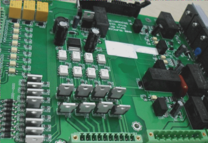
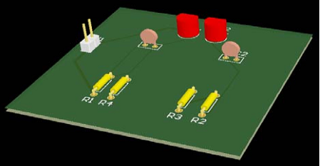
– **Assembly Drawing**: This provides detailed information about the position and orientation of components on both sides of the PCB. It highlights the placement of components and their alignment, ensuring that assembly processes can be accurately performed.
– **Component Placement Files**: These files are specifically designed for automated component placement systems, such as robotic pick-and-place machines. They guide these systems in the precise placement of components on the board, ensuring accuracy and efficiency in the assembly process.
### 2. **File Output**
– **Composite Drawing Files**: These comprehensive files include a full assembly view of the finished PCB, showcasing both the components and the underlying circuit connections. This serves as a clear reference for manufacturers during production.
– **3D View Files**: With 3D rendering capabilities, these files provide a three-dimensional representation of the PCB. They help visualize the board’s structure, aiding in both design verification and the preparation for 3D printing or other prototyping methods.
### Conclusion
These output files are integral to the seamless transition from design to physical production. Altium Designer’s ability to generate a variety of formats ensures that every aspect of the PCB’s lifecycle—from assembly to final inspection—is fully covered, catering to the different needs of PCB manufacturers and assembly systems.
### PCB Design Output Files and Reports: A Comprehensive Guide
The PCB design process involves creating various output files and reports to facilitate manufacturing. These outputs contain critical information such as layer details, drilling data, component lists, and more. Understanding how to generate these files efficiently is essential for smooth transition from design to production. In this guide, we will explore the different types of output files in PCB design, including Gerber files, drill files, BOMs (Bill of Materials), and other important documentation.
#### 1. **Schematic Design Outputs**
– **Schematic Diagram (Print)**: This represents the layout of the components and their interconnections. It’s the foundational blueprint for the PCB design.
– **Composite Drilling Diagram**: This diagram combines information about the size and locations of drill holes. It provides a comprehensive view of the drilling requirements on the PCB.
– **Demonstration and Guide Drilling Diagrams**: Multiple diagrams may be required to demonstrate drilling locations and sizes in different orientations or layers.
– **Final Drawing Output**: This is the consolidated drawing that combines all production files (e.g., Gerber, drill files, etc.) into a final output package, ready for manufacturing.
#### 2. **Gerber and Drill Files**
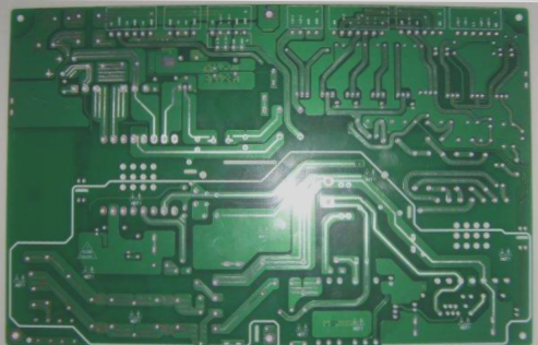
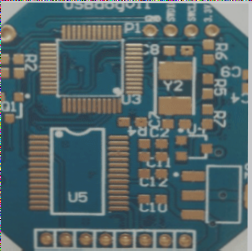
– **Gerber Files**: These files are essential for PCB fabrication, containing detailed layer information (such as signal layers, solder mask, and copper layers). Each layer is stored as a separate Gerber file, ensuring accurate reproduction during manufacturing.
– To generate Gerber files:
– Go to **File > Fabrication Outputs > Gerber Files**.
– In the dialog box, select the **Layers tab**, choose the layers to include, and click **OK** to accept default settings.
– Once generated, the Gerber files will be saved in the **Project Outputs** folder.
– **NC Drill Files**: These files contain hole-drilling data and are critical for CNC drilling machines during PCB manufacturing.
– To create these files, select **File > Fabrication Outputs > NC Drill Files**, and follow the setup prompts for hole type and drill data.
#### 3. **ODB++ Format**
– **ODB++ Files**: An advanced format that consolidates all manufacturing data into a single, database-like file. This format is useful for more complex designs and can streamline the communication between design and manufacturing teams.
#### 4. **Specialized Outputs**
– **Power-Plane Prints**: These are multi-layer drawings that represent internal power and ground planes, as well as their division across different layers of the PCB.
– **Solder and Paste Mask Prints**: These files detail the areas where solder mask and paste mask are applied, ensuring correct placement of solder and paste during assembly.
– **Test Point Report**: A report that highlights all test points on the PCB design, essential for quality control and testing.
#### 5. **Network List and Reports**
– **Netlist**: This file describes the connections between components, providing a comprehensive overview of the design’s electrical connections. It’s crucial for both design verification and transferring the design to other systems.
– **Bill of Materials (BOM)**: The BOM lists all the components used in the design, including part numbers, descriptions, and quantities. It is essential for sourcing and assembly.
– To generate a BOM:
1. Navigate to **Reports > Bill of Materials**.
2. Customize the BOM output by selecting the necessary columns and grouping criteria (e.g., by footprint).
3. Choose **CSV** format for export and click **Export** to generate the BOM.
– **Component Cross-Reference Report**: This report lists the components in a cross-referenced format, based on the original schematic design.
– **Project Hierarchy Report**: This report shows the structure of the entire PCB project, outlining the different files and documents associated with the design.
– **Single Pin Nets Report**: This generates a list of any nets that are connected to only one component pin, which can help identify potential design issues.
– **Simple BOM**: A simplified version of the BOM, typically in text or CSV format, for quick reference.
#### 6. **Output Job Files and Automation**
Many of the output files in PCB design are repetitive, especially across multiple projects. To streamline this, **Output Job Files** can be used in software like Altium Designer. The Output Job Editor allows you to bundle multiple output files into a single job, automating the process of generating and exporting all necessary files in one go.
#### 7. **Manual Output File Generation**
In the final stage of PCB design, output files can be generated manually, particularly when you want full control over the process or are not using the Output Job Editor.
– **Generating Gerber Files**:
– Navigate to **File > Fabrication Outputs > Gerber Files** and configure the layers as needed.
– Each Gerber file corresponds to a specific layer (top, bottom, signal, etc.) and will be saved with an appropriate extension (e.g., `.gto` for Top Overlay).
– **Creating NC Drill Files**:
– Similar to Gerber files, select **File > Fabrication Outputs > NC Drill Files** to generate the necessary drilling data for the CNC machine.
– **Creating BOM**:
– Use **Reports > Bill of Materials** to generate a BOM, choosing the appropriate columns and export format (typically CSV).
#### 8. **Conclusion**
The successful creation and output of PCB design files require attention to detail and proper setup. Gerber files, drill files, BOMs, and other specialized reports ensure that the design can be accurately manufactured and assembled. Tools like Output Job Files in Altium Designer help streamline the process, saving time and reducing errors. As you progress through more designs, you will become more efficient at using these output files and may find yourself reusing similar output configurations for each new project.