Currently, many people perceive the PCB manufacturing process as overly complex and difficult to understand. However, in reality, the process is not as challenging as it seems once you break it down. So, what should you do if you find the process daunting? A practical solution is to directly reach out to Wanlong Lean, a trusted provider for multi-layer PCB production. Let’s simplify the steps and offer you useful tips on how multi-layer PCBs are made. It’s not as hard as you might think—keep reading for a clearer understanding!
In general, PCB manufacturing follows a subtractive method, which involves removing excess copper foil from the base copper-clad board to create the desired conductive patterns. This subtractive process is primarily done using chemical etching, which is one of the most cost-effective and efficient methods available.
The etching process only targets the unprotected copper areas, so the conductive patterns need to be shielded. To protect these areas, a resist layer is applied over the desired conductive pattern before the etching process begins. This ensures that the copper that should remain intact stays protected while the unwanted copper is effectively removed through chemical corrosion.

In the early stages of printed circuit board (PCB) manufacturing, circuit patterns were created using screen printing, and the process was referred to as “printed circuit.” However, as electronic products became more complex, the resolution of printed circuits no longer met the growing demands of the industry. This led to the adoption of photoresist materials, which significantly improved the precision of circuit patterning.
**Photoresist Technology and Its Role**
Photoresist is a light-sensitive material that undergoes a photochemical reaction when exposed to light of a specific wavelength. This reaction causes the photoresist to polymerize, forming a protective layer. By using a pattern film, the resist can be selectively exposed, and the unexposed portions are removed by a developer solution (typically a diluted solution of carbonic acid or sodium hydroxide), leaving behind the desired pattern. This technology allowed for far more precise circuit creation compared to traditional screen printing.
**Through-Hole Metallization for Interlayer Conduction**
To enable electrical connections between different layers of the PCB, metallized holes are used. These holes are drilled into the board and then electroplated with metal, usually copper, to form conductive pathways between layers. This process is essential for achieving the interlayer electrical connections that are characteristic of multi-layer PCBs.
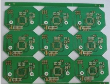
**Conventional 6-Layer PCB Production Process**
The production of a typical 6-layer PCB involves several key steps:
1. **Preparation of Inner Layers**
– **Cutting and Lamination:** Begin with raw double-sided copper-clad laminates. These are cut to size and then a pattern resist layer is applied to the inner surface to define the circuit layout.
– **Inner Layer Etching:** The copper foil is then etched away from the areas not protected by the resist, creating the required circuit pattern on the inner layers.
2. **Layer Stacking and Lamination**
– The two inner core layers are then aligned and bonded using an epoxy resin glass fiber prepreg. The prepreg serves as an intermediate layer that holds the cores together.
– The assembly is then subjected to high temperature and pressure in a press, which causes the resin in the prepreg to flow, bond the layers, and cure, solidifying the structure. The prepreg is a semi-cured material that, when heated, undergoes a chemical reaction with the curing agent, becoming solid and ensuring a strong bond between the layers.
3. **Outer Layer Processing**
– **Drilling:** Holes for vias (electrical connections between layers) are drilled through the PCB.
– **Copper Plating:** The drilled holes are then copper-plated to ensure electrical conductivity between layers.
– **Outer Layer Patterning:** A resist layer is applied to the outer surfaces, which is then exposed to a pattern and etched to form the outer circuitry.
– **Solder Mask Application:** A solder mask (typically green) is applied to protect the copper traces and prevent solder bridges during assembly. Additional details, such as text or component identification, may be printed on this layer.
– **Surface Finishing:** To protect the exposed copper and improve solderability, surface finishes like tin spraying or immersion gold are applied to the board.
– **Final Shaping:** The PCB is then cut or milled to its final dimensions.
Through this structured and methodical process, a high-quality, multi-layer PCB is created, capable of meeting the demands of increasingly sophisticated electronic devices. Each step, from photoresist application to drilling, plating, and surface finishing, ensures that the PCB performs reliably in its intended applications.
In general, PCB manufacturing follows a subtractive method, which involves removing excess copper foil from the base copper-clad board to create the desired conductive patterns. This subtractive process is primarily done using chemical etching, which is one of the most cost-effective and efficient methods available.
The etching process only targets the unprotected copper areas, so the conductive patterns need to be shielded. To protect these areas, a resist layer is applied over the desired conductive pattern before the etching process begins. This ensures that the copper that should remain intact stays protected while the unwanted copper is effectively removed through chemical corrosion.
In the early stages of printed circuit board (PCB) manufacturing, circuit patterns were created using screen printing, and the process was referred to as “printed circuit.” However, as electronic products became more complex, the resolution of printed circuits no longer met the growing demands of the industry. This led to the adoption of photoresist materials, which significantly improved the precision of circuit patterning.
**Photoresist Technology and Its Role**
Photoresist is a light-sensitive material that undergoes a photochemical reaction when exposed to light of a specific wavelength. This reaction causes the photoresist to polymerize, forming a protective layer. By using a pattern film, the resist can be selectively exposed, and the unexposed portions are removed by a developer solution (typically a diluted solution of carbonic acid or sodium hydroxide), leaving behind the desired pattern. This technology allowed for far more precise circuit creation compared to traditional screen printing.
**Through-Hole Metallization for Interlayer Conduction**
To enable electrical connections between different layers of the PCB, metallized holes are used. These holes are drilled into the board and then electroplated with metal, usually copper, to form conductive pathways between layers. This process is essential for achieving the interlayer electrical connections that are characteristic of multi-layer PCBs.
**Conventional 6-Layer PCB Production Process**
The production of a typical 6-layer PCB involves several key steps:
1. **Preparation of Inner Layers**
– **Cutting and Lamination:** Begin with raw double-sided copper-clad laminates. These are cut to size and then a pattern resist layer is applied to the inner surface to define the circuit layout.
– **Inner Layer Etching:** The copper foil is then etched away from the areas not protected by the resist, creating the required circuit pattern on the inner layers.
2. **Layer Stacking and Lamination**
– The two inner core layers are then aligned and bonded using an epoxy resin glass fiber prepreg. The prepreg serves as an intermediate layer that holds the cores together.
– The assembly is then subjected to high temperature and pressure in a press, which causes the resin in the prepreg to flow, bond the layers, and cure, solidifying the structure. The prepreg is a semi-cured material that, when heated, undergoes a chemical reaction with the curing agent, becoming solid and ensuring a strong bond between the layers.
3. **Outer Layer Processing**
– **Drilling:** Holes for vias (electrical connections between layers) are drilled through the PCB.
– **Copper Plating:** The drilled holes are then copper-plated to ensure electrical conductivity between layers.
– **Outer Layer Patterning:** A resist layer is applied to the outer surfaces, which is then exposed to a pattern and etched to form the outer circuitry.
– **Solder Mask Application:** A solder mask (typically green) is applied to protect the copper traces and prevent solder bridges during assembly. Additional details, such as text or component identification, may be printed on this layer.
– **Surface Finishing:** To protect the exposed copper and improve solderability, surface finishes like tin spraying or immersion gold are applied to the board.
– **Final Shaping:** The PCB is then cut or milled to its final dimensions.
Through this structured and methodical process, a high-quality, multi-layer PCB is created, capable of meeting the demands of increasingly sophisticated electronic devices. Each step, from photoresist application to drilling, plating, and surface finishing, ensures that the PCB performs reliably in its intended applications.