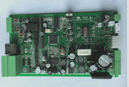
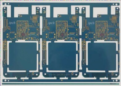
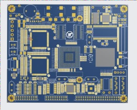
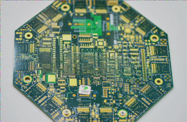
1. **Printed Circuit Board Design Requirements**
1. **Correct**
This is the most fundamental and critical requirement for printed circuit board design. It ensures the accurate realization of the electrical schematic diagram and avoids fatal errors such as “short circuit” and “open circuit.” Achieving this basic requirement can be challenging in manual design and with simple CAD software. Typically, products require more than two rounds of trial production and modification. Advanced CAD software with inspection functions helps to ensure the electrical correctness of the connections.
2. **Reliable**
This represents a higher level of PCB design requirements. A correctly connected circuit board is not necessarily reliable. Issues like inappropriate board selection, incorrect board thickness, improper installation, and poor component layout can lead to unreliable operation, early failure, or complete malfunction. For instance, while multi-layer boards are more complex to design than single or double-layer boards, they are not always as reliable. Generally, simpler structures, smaller use surfaces, fewer board layers, and simpler designs enhance reliability.
3. **Reasonable**
This is a more intricate and challenging requirement in PCB design. The entire lifecycle of a printed circuit board—from manufacturing and inspection to assembly, debugging, usage, and maintenance—is influenced by the board’s reasonableness. Difficulties such as complex board shapes, small lead holes, challenging assembly, or improper maintenance can increase costs and extend working hours. These issues often stem from design mistakes. While there is no absolutely reasonable design, continual improvement and rationalization are essential. This process demands the designer’s sense of responsibility, rigorous approach, and practical experience.

4. Economy
This goal is neither particularly easy nor particularly difficult, but it is essential to achieve. To make it “easier,” choose low-cost boards, minimize board size, use direct-welded wires for connections, select the cheapest surface coating, and opt for the lowest-priced processing plant. These measures can reduce the manufacturing cost of the printed board. However, be aware that these cost-saving choices may lead to poor workmanship and reduced reliability, potentially increasing both manufacturing and maintenance costs. Consequently, achieving true economic efficiency is challenging. The principle of market competition dictates that even products with advanced principles and high technology can fail due to economic reasons.
PCB Experience:
1. There must be a reasonable layout: such as separating input/output, AC/DC, strong/weak signals, high/low frequency, and high/low voltage. Their orientations should be linear (or separated) to prevent mutual interference. The ideal arrangement is a straight line, though this is often difficult to achieve. The least favorable arrangement is a circular one, though isolation techniques can help improve it. For DC, small signal, and low voltage PCBs, design requirements can be less stringent. Thus, “reasonable” is a relative term.
Problems that arise during post-production are often due to PCB design issues, such as excessive vias and potential issues with the copper sinking process, which can create hidden problems. Therefore, design should aim to minimize the number of vias. A high density of parallel lines in the same direction can lead to soldering issues, so line density should match the soldering process level. Small distances between solder joints can complicate manual soldering and affect quality. Therefore, the minimum distance between solder joints should balance the quality and efficiency of the soldering personnel. Small pad sizes or mismatched pad and hole sizes can hinder manual or CNC drilling. Thin wires and large unwired areas without copper are prone to uneven corrosion, potentially leading to wire breakage. Proper copper setting is crucial not only for increasing the ground wire area but also for anti-interference.
2. Protel Print Settings
The print settings for SCH are relatively straightforward. Set all margins (Top, Bottom, Left, Right) to 0 and click Refresh to maximize the page area and enlarge the printed SCH image.
For PCB settings: Open File > Setup Printer… to configure printing options.
In the Printer Setup menu, select your printer. The first options are default printers, followed by installed printers; one suffix indicates Final and the other Composite. The Final option prints one layer at a time, while Composite prints all selected layers simultaneously. Choose based on your needs. Click the Options button to configure properties. If you select Final, you generally don’t need to adjust the options. Scale represents the printing ratio, defaulting to 1:1. For full-page printing, check the appropriate box. The “Show Hole” option on the right is crucial; select it to include holes on the circuit board. After setting up the paper size, finalize printer options. Then, return to the printer properties dialog, select Layers, and configure the printing layers. Adjust as needed based on your requirements.
3. Commonly Used PCB Library Files
1. The component library in the librarypcbconnectors directory contains most PCB packages for connector components:
1) **D type connectors.ddb** – Contains packages for parallel and serial port interface components.
2) **headers.ddb** – Contains packages for various plug components.
2. The component library in the librarypcbgeneric footprints directory includes most PCB packages for common components.
1. **Correct**
This is the most fundamental and critical requirement for printed circuit board design. It ensures the accurate realization of the electrical schematic diagram and avoids fatal errors such as “short circuit” and “open circuit.” Achieving this basic requirement can be challenging in manual design and with simple CAD software. Typically, products require more than two rounds of trial production and modification. Advanced CAD software with inspection functions helps to ensure the electrical correctness of the connections.
2. **Reliable**
This represents a higher level of PCB design requirements. A correctly connected circuit board is not necessarily reliable. Issues like inappropriate board selection, incorrect board thickness, improper installation, and poor component layout can lead to unreliable operation, early failure, or complete malfunction. For instance, while multi-layer boards are more complex to design than single or double-layer boards, they are not always as reliable. Generally, simpler structures, smaller use surfaces, fewer board layers, and simpler designs enhance reliability.
3. **Reasonable**
This is a more intricate and challenging requirement in PCB design. The entire lifecycle of a printed circuit board—from manufacturing and inspection to assembly, debugging, usage, and maintenance—is influenced by the board’s reasonableness. Difficulties such as complex board shapes, small lead holes, challenging assembly, or improper maintenance can increase costs and extend working hours. These issues often stem from design mistakes. While there is no absolutely reasonable design, continual improvement and rationalization are essential. This process demands the designer’s sense of responsibility, rigorous approach, and practical experience.
4. Economy
This goal is neither particularly easy nor particularly difficult, but it is essential to achieve. To make it “easier,” choose low-cost boards, minimize board size, use direct-welded wires for connections, select the cheapest surface coating, and opt for the lowest-priced processing plant. These measures can reduce the manufacturing cost of the printed board. However, be aware that these cost-saving choices may lead to poor workmanship and reduced reliability, potentially increasing both manufacturing and maintenance costs. Consequently, achieving true economic efficiency is challenging. The principle of market competition dictates that even products with advanced principles and high technology can fail due to economic reasons.
PCB Experience:
1. There must be a reasonable layout: such as separating input/output, AC/DC, strong/weak signals, high/low frequency, and high/low voltage. Their orientations should be linear (or separated) to prevent mutual interference. The ideal arrangement is a straight line, though this is often difficult to achieve. The least favorable arrangement is a circular one, though isolation techniques can help improve it. For DC, small signal, and low voltage PCBs, design requirements can be less stringent. Thus, “reasonable” is a relative term.
Problems that arise during post-production are often due to PCB design issues, such as excessive vias and potential issues with the copper sinking process, which can create hidden problems. Therefore, design should aim to minimize the number of vias. A high density of parallel lines in the same direction can lead to soldering issues, so line density should match the soldering process level. Small distances between solder joints can complicate manual soldering and affect quality. Therefore, the minimum distance between solder joints should balance the quality and efficiency of the soldering personnel. Small pad sizes or mismatched pad and hole sizes can hinder manual or CNC drilling. Thin wires and large unwired areas without copper are prone to uneven corrosion, potentially leading to wire breakage. Proper copper setting is crucial not only for increasing the ground wire area but also for anti-interference.
2. Protel Print Settings
The print settings for SCH are relatively straightforward. Set all margins (Top, Bottom, Left, Right) to 0 and click Refresh to maximize the page area and enlarge the printed SCH image.
For PCB settings: Open File > Setup Printer… to configure printing options.
In the Printer Setup menu, select your printer. The first options are default printers, followed by installed printers; one suffix indicates Final and the other Composite. The Final option prints one layer at a time, while Composite prints all selected layers simultaneously. Choose based on your needs. Click the Options button to configure properties. If you select Final, you generally don’t need to adjust the options. Scale represents the printing ratio, defaulting to 1:1. For full-page printing, check the appropriate box. The “Show Hole” option on the right is crucial; select it to include holes on the circuit board. After setting up the paper size, finalize printer options. Then, return to the printer properties dialog, select Layers, and configure the printing layers. Adjust as needed based on your requirements.
3. Commonly Used PCB Library Files
1. The component library in the librarypcbconnectors directory contains most PCB packages for connector components:
1) **D type connectors.ddb** – Contains packages for parallel and serial port interface components.
2) **headers.ddb** – Contains packages for various plug components.
2. The component library in the librarypcbgeneric footprints directory includes most PCB packages for common components.

