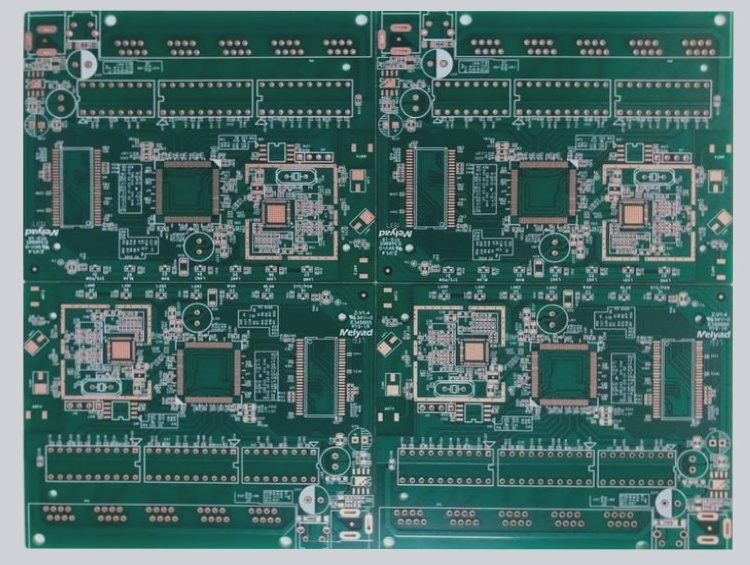
1. The PCB consists of various components and employs a range of complex processing techniques. It can have a single-layer, double-layer, or multi-layer structure, with each type requiring distinct production methods.
2. A printed circuit board is primarily made up of pads, vias, mounting holes, traces, components, connectors, fill areas, and electrical boundaries. Each of these elements serves specific functions:
3. Pad: A metal area designed for soldering the pins of components.
4. Via: A metal-lined hole used to establish connections between component pins on different layers.
5. Mounting hole: A hole used for securing the printed circuit board in place.

1. Wire: The copper film of the electrical network used to connect the pins of the components.
2. Connectors: Components used to connect circuit boards together.
3. Filling: Copper coating for the ground wire network, which effectively reduces impedance.
4. Electrical boundary: Defines the size of the circuit board; all components on the board must stay within this boundary.
5. Second, the common layer structures of printed circuit boards include three types: single-layer PCB, double-layer PCB, and multi-layer PCB. A brief description of these three layer structures is as follows:
6. (1) Single-layer board: A circuit board with copper on one side and none on the other. Components are usually placed on the side without copper, while the copper side is primarily used for wiring and soldering.
7. (2) Double-layer board: A circuit board with copper on both sides, typically referred to as the top layer and the bottom layer. Generally, the top layer is used for placing components, while the bottom layer is used for soldering.
8. (3) Multi-layer board: A circuit board with multiple working layers. In addition to the top and bottom layers, it contains several intermediate layers, which can serve as wiring layers, signal layers, power layers, and ground layers. These layers are insulated from each other, and connections between them are typically made through vias.
9. Third, the printed circuit board comprises various types of working layers, such as signal layers, protective layers, silk screen layers, and internal layers. The functions of each layer are briefly introduced as follows:
10. (1) Signal layer: Primarily used for placing components or routing. Protel DXP typically includes 30 middle layers, labeled Mid Layer1 through Mid Layer30. The middle layers are used for signal routing, while the top and bottom layers are used for component placement or copper deposition.
11. (2) Protective layer: Ensures that areas of the circuit board that do not need tinning remain untinned, thereby maintaining the reliability of the circuit board’s operation.
12. (3) Silk screen layer: Used to print serial numbers, production numbers, company names, and other identifiers on the PCB.
13. (4) Internal layer: Primarily serves as a signal routing layer. The CCP includes 16 internal layers.
14. (5) Other layers: Mainly include four types of layers.
15. Drill Guide (drilling azimuth layer): Used to indicate the positions for drilling holes on the printed circuit board.
2. A printed circuit board is primarily made up of pads, vias, mounting holes, traces, components, connectors, fill areas, and electrical boundaries. Each of these elements serves specific functions:
3. Pad: A metal area designed for soldering the pins of components.
4. Via: A metal-lined hole used to establish connections between component pins on different layers.
5. Mounting hole: A hole used for securing the printed circuit board in place.

1. Wire: The copper film of the electrical network used to connect the pins of the components.
2. Connectors: Components used to connect circuit boards together.
3. Filling: Copper coating for the ground wire network, which effectively reduces impedance.
4. Electrical boundary: Defines the size of the circuit board; all components on the board must stay within this boundary.
5. Second, the common layer structures of printed circuit boards include three types: single-layer PCB, double-layer PCB, and multi-layer PCB. A brief description of these three layer structures is as follows:
6. (1) Single-layer board: A circuit board with copper on one side and none on the other. Components are usually placed on the side without copper, while the copper side is primarily used for wiring and soldering.
7. (2) Double-layer board: A circuit board with copper on both sides, typically referred to as the top layer and the bottom layer. Generally, the top layer is used for placing components, while the bottom layer is used for soldering.
8. (3) Multi-layer board: A circuit board with multiple working layers. In addition to the top and bottom layers, it contains several intermediate layers, which can serve as wiring layers, signal layers, power layers, and ground layers. These layers are insulated from each other, and connections between them are typically made through vias.
9. Third, the printed circuit board comprises various types of working layers, such as signal layers, protective layers, silk screen layers, and internal layers. The functions of each layer are briefly introduced as follows:
10. (1) Signal layer: Primarily used for placing components or routing. Protel DXP typically includes 30 middle layers, labeled Mid Layer1 through Mid Layer30. The middle layers are used for signal routing, while the top and bottom layers are used for component placement or copper deposition.
11. (2) Protective layer: Ensures that areas of the circuit board that do not need tinning remain untinned, thereby maintaining the reliability of the circuit board’s operation.
12. (3) Silk screen layer: Used to print serial numbers, production numbers, company names, and other identifiers on the PCB.
13. (4) Internal layer: Primarily serves as a signal routing layer. The CCP includes 16 internal layers.
14. (5) Other layers: Mainly include four types of layers.
15. Drill Guide (drilling azimuth layer): Used to indicate the positions for drilling holes on the printed circuit board.

