Enhancing PCB Quality and Reliability: Common Failure Analysis Techniques
- 1. Appearance Inspection
- 2. X-ray Fluoroscopy Inspection
- 3. Slice Analysis
- 4. Scanning Acoustic Microscope Analysis
- 5. Microscopic Infrared Analysis
- 6. Scanning Electron Microscope Analysis
- 7. X-ray Energy Spectrum Analysis
- 8. Photoelectron Spectroscopy (XPS)
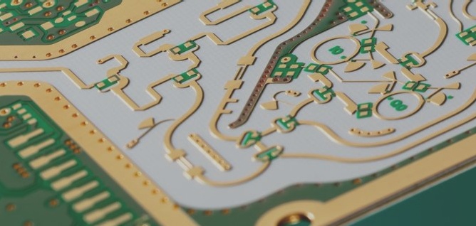
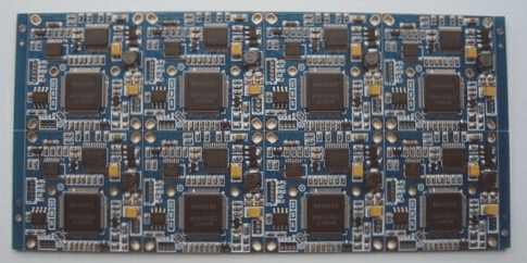
Visual inspection and the use of instruments like stereo microscopes and magnifying glasses are essential to identify PCB board exterior issues such as pollution, corrosion, and circuit layout irregularities.
X-ray systems help detect internal defects within PCB board through-holes, including solder joint defects and through-hole faults, enhancing inspection capabilities.
By providing cross-sectional views of PCB structures, slice analysis offers detailed microstructural information crucial for quality assessment and subsequent enhancements.
This method detects defects in electronic assemblies and packaging by utilizing high-frequency ultrasound reflections to image amplitude, phase, and polarity changes.
Combining infrared spectroscopy with microscopy, this analysis identifies trace organic contaminants affecting PCB pad solderability or lead pin connections.
SEM generates high-resolution images revealing surface topography and elemental composition, crucial for observing pad surfaces, solder joint metallography, and tin whisker analyses.
Integrated with SEM, X-ray energy spectrometers detect characteristic X-rays emitted when high-energy electron beams strike sample surfaces, enabling elemental analysis based on atomic energy level differences.
XPS analyzes surface atoms by irradiating samples with X-rays to measure emitted electrons’ kinetic energies, identifying elements and their chemical states crucial for analyzing PCB pad coatings and contaminants.
Latest Updates:
Advancements in PCB manufacturing now include the use of artificial intelligence algorithms to predict failure modes and improve quality control processes. Additionally, the integration of Internet of Things (IoT) technology allows for real-time monitoring of PCB performance and detection of potential issues before they escalate.

Thermal Analysis
Thermal analysis plays a critical role in evaluating the reliability of PCBs by assessing key thermal properties. Two common techniques used in this process are:
- Differential Scanning Calorimetry (DSC): DSC measures the thermal energy differences between sample and reference materials at controlled temperatures. This method is essential for understanding PCB polymer curing and glass transition temperatures, which are crucial for ensuring the reliability of the board.
- Thermal Mechanical Analysis (TMA): TMA measures the deformations of materials under controlled temperature or mechanical stress conditions. This technique is vital for evaluating PCB expansion coefficients and glass transition temperatures, especially in the context of industry trends that prioritize high-density, lead-free, and halogen-free PCB designs.
By utilizing thermal analysis techniques such as DSC and TMA, PCB experts can make informed decisions to enhance the performance and reliability of printed circuit boards in line with evolving industry requirements.


