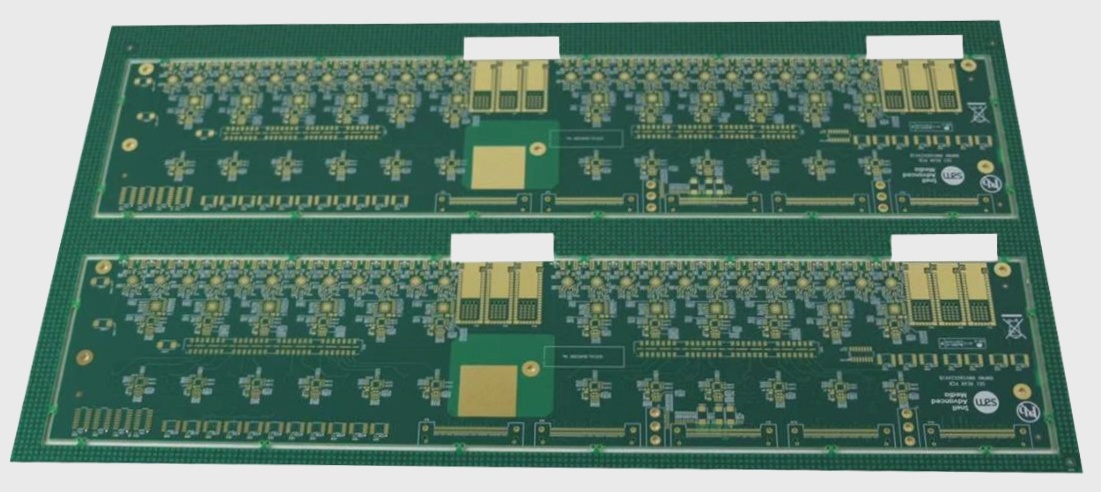
The Evolution of China’s PCB Industry
China’s PCB industry has undergone remarkable growth since its establishment in 1956, evolving into a robust sector by the late 1970s. The country laid the foundation for its PCB industry from 1963 to 1978 and experienced accelerated development after implementing reform and opening-up policies. This progress was fueled by the integration of advanced foreign technologies and equipment, leading to the rapid production of single-layer, double-sided, and multilayer boards.
The domestic PCB sector, initially small-scale, expanded significantly due to the concentration of downstream industries and cost advantages in labor and land. By 2002, China became the world’s third-largest PCB producer, surpassing the United States in 2003 with an output value exceeding USD 6 billion. China’s global PCB output share grew from 8.54% in 2000 to 15.30% in 2003, positioning the country as a key player in the industry. By 2006, China had surpassed Japan in output value and emerged as a global hub for PCB production and technology.
In recent years, China’s PCB industry has maintained an impressive annual growth rate of around 20%, outpacing global industry growth and solidifying its position as a dominant force in the global market.
Flying Pin Testing: Revolutionizing PCB Testing
Flying pin testing has revolutionized the PCB testing process, offering solutions to challenges associated with traditional methods. This innovative testing technique utilizes fast-moving electrical probes, driven by motors, to make contact with device pins and conduct electrical measurements. Unlike conventional needle bed testing, flying pin testing employs dynamic probes that swiftly traverse the PCB surface, enhancing testing efficiency.
Originally designed for bare board testing, flying pin testing now supports complex applications like online simulation testing, thanks to advancements in hardware and software. Real-time testing capabilities have significantly enhanced PCB testing efficiency, reducing development time from weeks to hours, particularly for low-yield and quick-turn assembly products. This innovation accelerates product design cycles and time-to-market, playing a vital role in the competitive PCB manufacturing landscape.
Structural Features of the Flying Needle Test System
The flying needle test system represents an advanced iteration of the traditional needle bed in-circuit tester (ICT). It utilizes a high-speed X-Y mechanism with 4 heads and 8 probes to test PCBs. Probes, with a typical test gap of 0.2mm, make contact with test pads and vias on the unit under test (UUT), which is conveyed to the testing machine via a transport system. Each probe is linked to equipment like signal generators and sensors to test UUT components, shielding other parts to prevent interference. The system can identify faults such as shorts, open circuits, and component values, with an integrated camera aiding in component location, especially for polar capacitors.

The Flying Needle Test System: Revolutionizing PCB Assembly Testing
The flying needle test system offers high accuracy and repeatability, with probe positioning precision ranging from 5-15 microns. This precision enables accurate testing of small or densely packed Unit Under Tests (UUTs).
Latest Updates:
- Advanced Technology: Incorporating cutting-edge technology, the flying needle tester now provides even higher accuracy levels, ensuring precise testing results.
- Enhanced Efficiency: Recent upgrades have further optimized the testing process, reducing setup time and enhancing overall efficiency.
- Improved User Interface: The system now features a more user-friendly interface, simplifying operation for technicians.
Test Development and Debugging Made Easy
Programming a flying needle tester is quicker and simpler compared to traditional ICT systems. With tools like the Grpilot system by GenRad, test developers can convert CAD data into a usable format within 1-4 hours.
Key Points:
- Efficient Programming: The system streamlines the test development process, saving valuable time and resources.
- Comprehensive Debugging: Test developers can fine-tune the system for optimal performance, ensuring thorough test coverage.
- Quick Setup: The flying needle tester’s rapid setup minimizes downtime and accelerates the testing phase.
Advantages of the Flying Needle Test System
The flying needle test system offers numerous advantages over traditional ICT methods, including rapid test development, lower costs, flexibility, and quick feedback for designers.
Key Benefits:
- Rapid Test Development: Enables faster product development and testing.
- Cost-Effective: Reduces the need for expensive fixtures and specialized equipment.
- Flexibility: Ideal for low-volume and prototype PCB testing.
- Quick Feedback: Helps designers identify and resolve issues promptly.
Features and Software Support
The flying needle tester, such as the A3 model from AGT company, offers a testing area of 550 x 430mm with a plate thickness of 6mm. Key software tools like IGI, DPS Wizard, A3 Debugger, and A3 Test Player provide comprehensive support for data processing and test setup.
Software Highlights:
- IGI: Processes Gerber data and optimizes hole configurations for accurate testing.
- DPS Wizard: Generates position coordinates and panel layouts for effective scanning.
- A3 Debugger: Calibrates the system to maintain test accuracy over time.
- A3 Test Player: Controls the testing process, allowing operators to customize test modes and parameters.
Browser for PCB Testing
The browser is a crucial tool used to identify open or short circuits on a PCB, allowing for precise marking of their locations for further analysis.
Common Issues and Solutions
- If the DPS software fails to generate a test program, it may be due to misaligned data in IGI or incorrectly selected antenna points.
- Aligning data correctly, choosing the right antenna points, and adjusting the network size can help resolve these issues effectively.
Conclusion: PCB Testing in China
PCB testing in China is advancing, with companies like WellCircuits leading the way in innovation. WellCircuits utilizes cutting-edge automated production lines and testing equipment, including 60 flying needle testers and 4 AOI optical testers.
Since February 2012, the company has shifted to a fully automated testing process, eliminating testing fees and improving overall efficiency. The flying needle test system significantly accelerates PCB production and testing, offering manufacturers a cost-effective, adaptable, and swift solution for testing prototypes and low-volume production boards.


