1. **Simulation Operation of Preliminary Design**
To ensure the designed circuit functions correctly, computer software must first be used for simulation. This software can read the design files and visually display the circuit’s operation in various formats.
2. This approach is more efficient than creating a physical PCB prototype and measuring it manually.
3. The placement of components on the PCB is determined by their connections. Components must be routed in the most efficient manner possible. Efficient routing means minimizing the length of the trace and reducing the number of layers (which in turn lowers the number of vias). However, this is not always straightforward in practice, and we’ll address this issue later. Here’s what the bus looks like when routed on the PCB.
4. To achieve optimal routing for the components, placement is crucial. It influences the ability to test connections and ensure proper operation at high speeds. Modern software can check whether each component is correctly positioned and verify its functionality under high-speed conditions. This step is referred to as component placement, though we won’t go into it in great detail.

1. If there is an issue with the circuit design, you can adjust the placement of the components before finalizing the circuit layout for manufacturing.
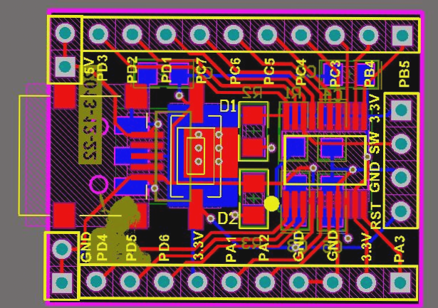
2. The connections in the exported PCB’s wiring overview now resemble field wiring. This step is typically fully automated, but some parts often require manual adjustments. The diagram represents a 2-layer floor design, with the red and blue lines indicating the component layer and solder layer, respectively. The white text with four squares marks the printed surface of the various signs. The red dots and circles indicate drilling and pilot holes. On the right, you can see the golden finger on the PCB’s soldering surface.
3. The final aspect of the PCB is often referred to as the “working film” (or artwork). Every design must adhere to a set of requirements, such as minimum clearance between traces, minimum trace width, and other practical limitations. These rules vary depending on factors such as circuit speed, signal strength, power consumption, noise sensitivity, as well as material quality and manufacturing capabilities. If the current increases, the trace width must also be increased. To reduce PCB costs while minimizing the number of layers, it is also important to ensure these regulations remain consistent.
4. When a design requires more than two layers, a power plane and a ground plane are typically added. These planes help prevent the transmission signals on the signal layer from being interfered with and can also serve as shields for the signal layer.
5. The rear circuit test is conducted to verify that the wiring functions correctly after it has been completed. This test can also identify any incorrect connections, with the overview showing all online connections.
6. Production documentation creation: Since many CAD tools are available for PCB design, manufacturers must have documentation that meets industry standards to produce circuit boards. Several standard specifications exist, with the Gerber file format being the most widely used.
7. A complete set of Gerber files includes the layout for each signal, power, and ground plane, the layout for the printed surface of the soldering layer, stencil data, and additional files for drilling and extraction.
8. Electromagnetic Compatibility (EMC) concerns: Electronic devices not designed in compliance with EMC standards may emit electromagnetic energy that interferes with nearby devices. EMC sets limits on electromagnetic interference (EMI), electromagnetic fields (EMF), and radio frequency interference (RFI), ensuring that nearby electrical devices operate correctly. EMC regulations strictly limit the energy emitted or transmitted to other devices and aim to reduce the magnetization from external EMF, EMI, and RFI. In essence, these regulations prevent electromagnetic energy from entering or exiting a device. This issue can be challenging to address. Common solutions include using power and ground planes or enclosing the PCB in a metal casing. Power and ground layers help shield the signal layer from interference, while a metal casing offers similar benefits.
9. We have not delved deeply into these issues. The maximum circuit speed is determined by the operating conditions defined by EMC regulations. Internal EMI, such as current depletion between conductors, increases with higher frequencies. If the gap between the conductors becomes too large, the distance between them must be extended. The regulations also dictate ways to avoid high voltage and minimize current consumption in the circuit. The signal delay rate is also crucial, with shorter trace lengths being preferable. Consequently, smaller PCBs with well-optimized routing are better suited for high-speed operation than larger ones.
To ensure the designed circuit functions correctly, computer software must first be used for simulation. This software can read the design files and visually display the circuit’s operation in various formats.
2. This approach is more efficient than creating a physical PCB prototype and measuring it manually.
3. The placement of components on the PCB is determined by their connections. Components must be routed in the most efficient manner possible. Efficient routing means minimizing the length of the trace and reducing the number of layers (which in turn lowers the number of vias). However, this is not always straightforward in practice, and we’ll address this issue later. Here’s what the bus looks like when routed on the PCB.
4. To achieve optimal routing for the components, placement is crucial. It influences the ability to test connections and ensure proper operation at high speeds. Modern software can check whether each component is correctly positioned and verify its functionality under high-speed conditions. This step is referred to as component placement, though we won’t go into it in great detail.
1. If there is an issue with the circuit design, you can adjust the placement of the components before finalizing the circuit layout for manufacturing.
2. The connections in the exported PCB’s wiring overview now resemble field wiring. This step is typically fully automated, but some parts often require manual adjustments. The diagram represents a 2-layer floor design, with the red and blue lines indicating the component layer and solder layer, respectively. The white text with four squares marks the printed surface of the various signs. The red dots and circles indicate drilling and pilot holes. On the right, you can see the golden finger on the PCB’s soldering surface.
3. The final aspect of the PCB is often referred to as the “working film” (or artwork). Every design must adhere to a set of requirements, such as minimum clearance between traces, minimum trace width, and other practical limitations. These rules vary depending on factors such as circuit speed, signal strength, power consumption, noise sensitivity, as well as material quality and manufacturing capabilities. If the current increases, the trace width must also be increased. To reduce PCB costs while minimizing the number of layers, it is also important to ensure these regulations remain consistent.
4. When a design requires more than two layers, a power plane and a ground plane are typically added. These planes help prevent the transmission signals on the signal layer from being interfered with and can also serve as shields for the signal layer.
5. The rear circuit test is conducted to verify that the wiring functions correctly after it has been completed. This test can also identify any incorrect connections, with the overview showing all online connections.
6. Production documentation creation: Since many CAD tools are available for PCB design, manufacturers must have documentation that meets industry standards to produce circuit boards. Several standard specifications exist, with the Gerber file format being the most widely used.
7. A complete set of Gerber files includes the layout for each signal, power, and ground plane, the layout for the printed surface of the soldering layer, stencil data, and additional files for drilling and extraction.
8. Electromagnetic Compatibility (EMC) concerns: Electronic devices not designed in compliance with EMC standards may emit electromagnetic energy that interferes with nearby devices. EMC sets limits on electromagnetic interference (EMI), electromagnetic fields (EMF), and radio frequency interference (RFI), ensuring that nearby electrical devices operate correctly. EMC regulations strictly limit the energy emitted or transmitted to other devices and aim to reduce the magnetization from external EMF, EMI, and RFI. In essence, these regulations prevent electromagnetic energy from entering or exiting a device. This issue can be challenging to address. Common solutions include using power and ground planes or enclosing the PCB in a metal casing. Power and ground layers help shield the signal layer from interference, while a metal casing offers similar benefits.
9. We have not delved deeply into these issues. The maximum circuit speed is determined by the operating conditions defined by EMC regulations. Internal EMI, such as current depletion between conductors, increases with higher frequencies. If the gap between the conductors becomes too large, the distance between them must be extended. The regulations also dictate ways to avoid high voltage and minimize current consumption in the circuit. The signal delay rate is also crucial, with shorter trace lengths being preferable. Consequently, smaller PCBs with well-optimized routing are better suited for high-speed operation than larger ones.

