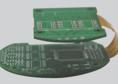
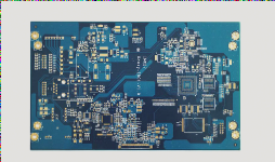
Printed Circuit Board Production Process
1. Print the Circuit Board
Print the designed circuit board using transfer paper, ensuring the shiny side is facing you. Print two circuit boards on one sheet and select the one with the best printing quality.
2. Cut the Copper Clad Laminate
Use a photosensitive plate to create a process diagram of the circuit board. Cut the copper clad laminate to match the circuit board size, avoiding excess to conserve materials.
3. Copper Clad Laminate Pretreatment
Polish the copper clad laminate surface with fine sandpaper to remove the oxide layer. This ensures effective adhesion of carbon powder during the circuit board transfer, aiming for a bright, stain-free surface.
4. Circuit Board Transfer
Trim the printed circuit board to size and adhere it to the copper clad laminate. Place the laminate in a heat transfer machine, ensuring alignment. After 2-3 cycles, the board should transfer securely. Preheat the machine to 160-200 degrees Celsius and handle with caution due to high temperatures.
Latest Update: Corrosion Process
After transferring, ensure the circuit board is complete. Use a black oil-based pen to repair any areas lacking transfer before proceeding with corrosion. Once the copper film is corroded, clean the board using a solution of hydrochloric acid, hydrogen peroxide, and water. Prioritize safety due to the corrosive nature of the solution.
PCB Drilling
Drilling the board is necessary for electronic components. Use appropriate drill bits based on pin thickness, maintaining high drill speed. Supervise operators closely during this process.
Circuit Board Treatment
After drilling, polish the board with sandpaper, rinse, and apply rosin. Solidify the rosin using a hot air blower for 2-3 minutes.
Double-Sided Plate Production Process
- Cutting
- Drilling
- Sinking Copper
- Line Creation
- Etching
- Solder Mask Application
- Character Addition
- Spray Tin or Heavy Gold Coating
- Edge Trimming
- V-Cut
- Flying Test
- Vacuum Packaging
Multi-Layer Plate Gold Plate Production Process
- Cutting
- Inner Layer Processing
- Lamination
- Drilling
- Sinking Copper
- Line Creation
- Etching
- Solder Mask Application
- Character Addition
- Edge Trimming
- V-Cut
- Flying Test
- Vacuum Packaging
Anatomy Process
- Remove components from the original board.
- Scan the board for a graphic file.
- Grind to access the intermediate layer.
- Scan the intermediate layer for another graphic file.
- Repeat steps 2-4 for all layers.
- Convert files to PCB diagrams using specialized software.
- Thoroughly check to complete the design.
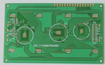
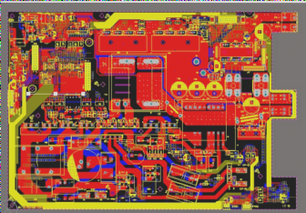
Layout Editor
Key details for layout design include single panels for cost efficiency, with the option for components or jumpers to bypass traces. Consider double panels if needed.
Double Panel PCB Fabrication Tips
- Double Panel PCBs can be used with or without plated through holes (PTH).
- PTH boards are more expensive and are best suited for complex, dense circuits.
- Minimize wires on the component side to make material access easier.
- In PTH boards, plated through holes are only for electrical connections, not for component installation.
- For cost-effectiveness and reliability, it’s advisable to limit the number of holes.
- When choosing between single-sided and double-sided PCBs, consider the component surface area (C) relative to the total PCB area (S) for optimal installation.
- Remember that “US” typically refers to one side’s area.
Understanding Pad Diameter and Maximum Wire Width
The relationship between pad diameter and maximum wire width is crucial in PCB fabrication, aluminum substrate, high-frequency board production, and more.
Relationship Chart:
- 0.040 inch / 40 Mil / 1.015 mm – 0.015 inch / 15 Mil / 0.38 mm
- 0.050 inch / 50 Mil / 1.27 mm – 0.020 inch / 20 Mil / 0.5 mm
- 0.062 inch / 62 Mil / 1.57 mm – 0.025 inch / 25 Mil / 0.63 mm
- 0.075 inch / 75 Mil / 1.9 mm – 0.025 inch / 25 Mil / 0.63 mm
- 0.086 inch / 86 Mil / 2.18 mm – 0.040 inch / 40 Mil / 1.01 mm
- 0.100 inch / 100 Mil / 2.54 mm – 0.040 inch / 40 Mil / 1.01 mm
- 0.125 inch / 125 Mil / 3.17 mm – 0.050 inch / 50 Mil / 1.27 mm
- 0.150 inch / 150 Mil / 3.81 mm – 0.075 inch / 75 Mil / 1.9 mm
- 0.175 inch / 175 Mil / 4.44 mm – 0.100 inch / 100 Mil / 2.54 mm
Key Production Considerations
- Ensure the circuit has been analyzed and basic units are used to smooth the signal.
- Check if short or isolated key leads are allowed in the circuit.
- Determine if shielding is necessary and effective.
- Utilize basic grid graphics effectively.
- Optimize the printed board size.
- Maximize selected wire widths and spacing.
- Employ optimal PCB pad and hole sizes.
- Review the appropriateness of photographic plates and sketches.
- Minimize the use of jumper wires and ensure they traverse components and accessories efficiently.
- Check the visibility, size, and correctness of letters post-assembly.
- Include windows on large copper foil areas to prevent blistering.
- Ensure tool positioning holes are included in the design.