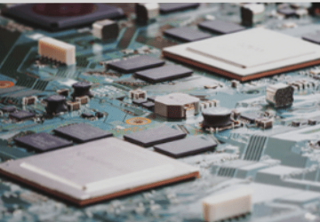
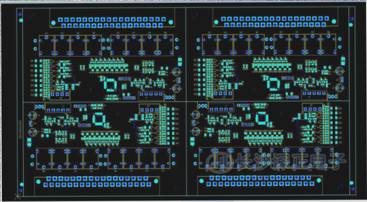
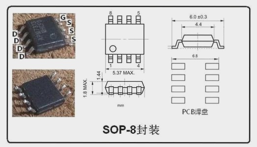
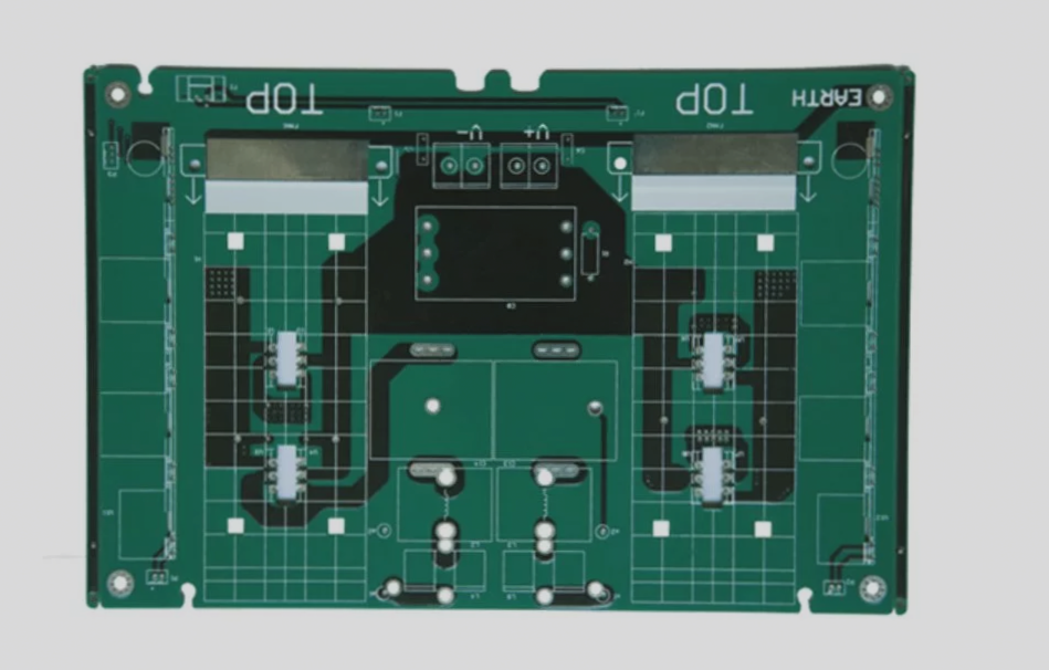
2. In a broad sense, SMT encompasses various components and devices. It includes surface mount components (SMC), surface mount devices (SMD), and surface mount printed circuit boards (SMB). These terms collectively describe the comprehensive PCB technology, which includes mixed printed circuit boards (PCB), dispensing, paste coating, surface mount equipment, component pick-and-place systems, soldering, and online testing.

1. Because SMC (Surface Mount Components) and SMD (Surface Mount Devices) minimize lead distribution characteristics and ensure strong soldering to the PCB surface, the parasitic capacitance and inductance between leads are significantly reduced. This greatly diminishes electromagnetic interference (EMI) and radio frequency interference (RFI), while improving high-frequency characteristics. Such components find extensive application in satellite communication products, such as low-noise down-frequency amplifiers (LNB) and other high-frequency devices used for ground-based satellite signal reception. PCBs utilized in high-frequency applications have specific electrical constant requirements. For instance, when the circuit operates below 109Hz, the PCB substrate’s electrical constant (X) typically needs to be less than 2.5.
2. Experimental findings indicate that the PCB substrate’s X value depends not only on its material characteristics but also on the content of reinforcing materials. Higher levels of reinforcement increase the X value, necessitating caution in their use for high-frequency PCBs. Excessive reinforcement can compromise the mechanical strength of these PCBs, which is critical given that some high-frequency products require ultra-thin PCBs, often only one-third the thickness of standard boards. This thinness makes them more susceptible to breakage, posing challenges in production.
3. Addressing these challenges, let’s discuss some practical insights and methods to overcome the fragility of thin PCBs used in high-frequency applications during surface mount production, thereby facilitating efficient mass production of such products.
4. The surface mount process primarily involves three key stages: solder paste application, component placement, and soldering. Here, we’ll focus on the first two stages.
5. In mass production, solder paste application is typically performed using fully automated printing machines. When a PCB enters such a machine for solder paste application, it needs to be securely fixed. Two common methods for fixing PCBs in the printing machine are using guide rails for conveyance and positioning, or employing vacuum suction under the guide rails for secure positioning.
6. For thin and fragile PCBs, during solder paste application, if the PCB is fixed using guide rails, it can lead to unintended bulging in the middle due to clamping forces. This not only increases the risk of PCB breakage but also results in uneven solder paste coating, adversely affecting coating quality across the PCB surface.


