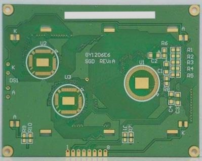
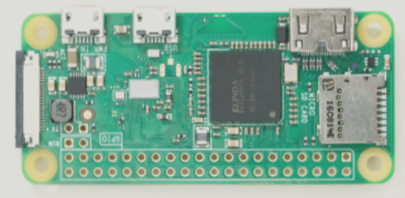
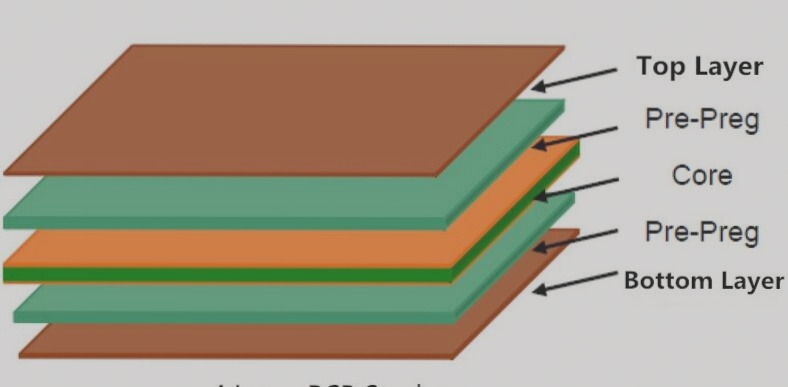
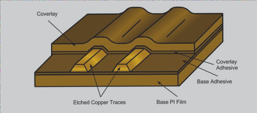
1. In today’s developed industry, PCB circuit boards are widely used in various electronic products. The color, shape, size, level, and materials of PCB circuit boards vary according to different industries. Therefore, clear information is essential in the design of PCB boards to avoid misunderstandings. This article summarizes ten major defects based on the PCB design process.
2. The Processing Level is Not Clearly Defined:
The single-sided board is designed on the TOP layer. If the front and back are not specified, it may be difficult to solder the components onto the board.
3. The Large Area of Copper Foil is Too Close to The Outer Frame:
The distance between the large area of copper foil and the outer frame should be at least 0.2mm or more. When milling the shape of the copper foil, insufficient distance can cause the copper foil to warp, leading to the solder resist falling off.
4. Drawing Pads with Filling Blocks:
Drawing pads with filler blocks may pass the DRC inspection during circuit design, but it is not conducive to processing. Therefore, similar pads cannot directly generate solder mask data. When solder resist is applied, the filler block area will be covered, resulting in difficulties in component welding.
5. The Electrical Ground Layer is Also a Patterned Pad and a Connection:
When designed as a patterned pad power supply, the ground layer is opposite to the actual printed board image. All connections are isolated lines. When drawing several sets of power or ground isolation lines, ensure there are no gaps; otherwise, short-circuiting of power supplies may occur, and this connection area cannot be blocked.
6. Random Characters:
The SMD soldering pad of the character cover pad brings inconvenience to the continuity test of the printed circuit board and component soldering. If the character design is too small, it makes screen printing difficult; if too large, characters may overlap, making it difficult to distinguish them.
6. The Surface Mount Device Pad is Too Short
For continuity testing, it is important to consider the spacing between pins on dense surface mount devices. The pads are often thin, making it necessary to install test pins in a staggered position. If the pad design is too short, it can hinder device installation but will allow for staggered test pin placement.
7. Single-Sided Pad Aperture Setting
When dealing with single-sided pads that are not drilled, it is crucial to mark drilled holes with a zero diameter to prevent issues with hole coordinates during data generation. Special markings should be used for single-sided pads that require drilling to ensure accuracy.
8. Pad Overlap
To prevent damage to the drill bit and holes, avoid overlapping holes during the drilling process, especially on multi-layer boards. Overlapping holes can lead to isolation disk errors on the negative film after drawing, resulting in scrap.
9. Excessive Filling Blocks or Thin Lines
When using filling blocks filled with thin lines in the design, there is a risk of losing or having incomplete gerber data. Drawing filling blocks with individual lines during light drawing data processing can create a large amount of data, making data processing more challenging.
10. Graphic Layer Misuse
Avoid creating unnecessary connections on graphic layers, as this can lead to confusion when designing multi-layer boards. The original design may have specified fewer layers, causing misunderstandings and violating conventional design practices. Keep graphic layers clear and intact during the design process to ensure accuracy.
These are some of the key defects to watch out for in PCB board design. By addressing these issues, you can improve production schedules and minimize errors in the PCB production process.