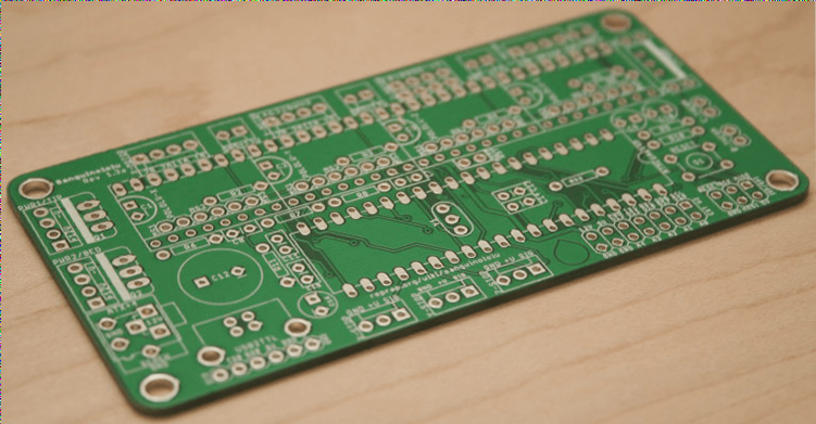
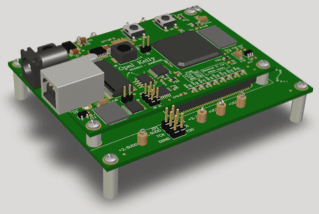
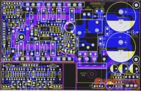
2. Below is an overview of some typical related processes. As this is a process introduction, it excludes circuit design, engineering drawings, and other production designs. Moreover, PCBs can be classified into different types, such as flexible boards, rigid boards, and rigid-flex boards. Based on the number of conductive layers, they can also be categorized as single-layer, double-layer, or four-layer boards. Here, we will focus on the manufacturing process of a typical four-layer rigid board.
3. The first step involves cutting the material. As the term implies, this step is about preparing the materials, which is quite straightforward. The purchased double-layer copper-clad laminate is cut to the size required for the working panel. For instance, if the initial dimensions are 1.5m x 1.8m, it may be cut into sections measuring 490mm x 800mm, suitable for the factory equipment. This operation utilizes a cutting machine, and after cutting, edging is performed to avoid swarf and scratches on the copper edges.

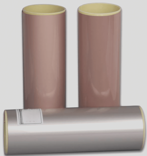
1. The material utilized is FR-4 copper-clad laminate. The copper foil has a thickness of 0.5 oz, approximately 18 µm. According to industry standards, when 1 ounce of copper is spread over 1 square inch, the foil thickness is about 36 µm. After etching, these copper foils form the PCB circuit. In the center lies a prepreg used for insulation and bonding, also referred to as PP, which is an epoxy or other resin impregnated into glass fiber cloth, providing flame-retardant insulation. PP materials come in various thicknesses, and during hot pressing, 1-2 sheets are used per the thickness requirements, following industry models such as 1080, 7628, etc.
2. This prepreg represents a critical material change. 5G communication products impose new demands for high heat dissipation, low dielectric constant, and low transmission loss, necessitating material modification and design adjustments.
3. The second step involves pre-treatment: the board is sent to the assembly line where dirt on the copper foil’s surface is cleaned with alkaline water, while acid water is used to remove oxides. This prepares the surface for better adhesion of the dry film in subsequent steps.
4. The third step is the production of the inner layer. It is termed the inner layer because the circuits of a four-layer board and two-layer copper foil are situated within the PCB stack. The entire process is controlled in a cleanroom environment classified to Class 1000. Equipment such as laminating machines, exposure machines, and wet etching lines are employed.
5. Initially, the dry photoresist film is applied. The exposure machine then emits a light source, allowing light to pass through the pre-designed circuit image to create a pattern on the photoresist surface.
6. Development and etching follow. After removing the residual photoresist, the circuit remains on the copper-clad board. Once complete, an AOI inspection is conducted to check for any line breaks or short circuits.
7. To enhance the bonding strength between the copper foil and the PP prepreg during the subsequent pressing process, browning treatment is performed to create copper oxide and cuprous oxide on the copper foil’s surface. At this stage, the inner layer production is complete.
8. The fourth step involves pressing, where the prepreg, laminated inner layer, and copper foil are combined to form a four-layer structure. A large flat-plate hot press is utilized. The primary component of PP is epoxy resin. Under tens of kilograms of pressure at approximately 150 degrees, and through heating and cooling for over an hour, the four-layer structure is achieved.
9. The fifth step, PCB drilling, involves using a high-speed drilling machine to create holes in the hot-pressed four-layer board according to the design specifications. Various diameters of through holes, semi-permeable blind holes, and precision holes for HDI high-density boards are produced, often employing laser machines for accuracy.
10. Additionally, aluminum foil is placed over the PCB during drilling to enhance heat dissipation and minimize debris. Some laminated wood chip boards are stacked underneath to ensure product flatness and prevent drill malfunctions.
11. The sixth step is copper plating for PTH, which coats the drilled holes with copper to facilitate electrical conduction between different copper foil layers.
12. The seventh step, plate plating, also known as one-time copper, aims to increase the thickness of the surface copper foil by plating an additional 6-8 µm.
13. The eighth step concerns the production of the outer layer circuit, which closely mirrors the inner layer process, involving dry film, exposure, development, and etching.
14. I believe this entire process exemplifies the classic procedure within the electronics industry. Whether for PCBs, touch screens, LCDs, or semiconductor chips, the underlying principles remain similar, with variations in accuracy at the millimeter, micrometer, and nanometer levels.
15. The ninth step, green oil solder mask application, is predominantly green, although some boards feature blue, red, yellow, or black. This is crucial as copper is prone to oxidation and scratches; thus, a protective layer of green ink is printed, baked, cured, and then exposed, developed, and washed, resulting in the board’s final appearance.
16. The tenth step involves printing white logos on the PCB. After the green oil is applied, these logos need to be printed.
17. The eleventh step, the tin-lead process, is applied to specific holes where connectors will be placed. Tin is sprayed to protect the copper foil and facilitate SMT surface mounting, while areas requiring better conductive contact, such as gold finger zones, are plated with nickel and gold for enhanced resistance to corrosion and wear. For instance, each hole and pad in the image below is treated with a tin spray at high temperatures in a hot air leveling furnace.
18. The twelfth step consists of shaping, where various forms, such as V-grooves, are milled into the working panel using a drill.
19. The above outlines a typical PCB production process. Finally, the boards undergo function testing, visual inspection, and packaging for shipment.


