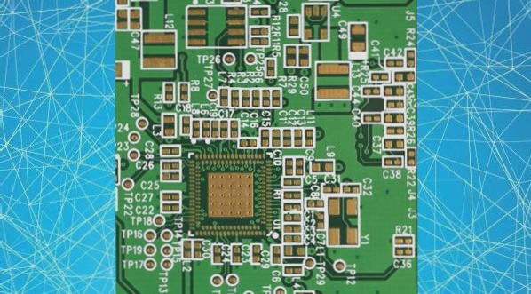
**What is PCB Film?**
The term “film” originally referred to a type of photographic material used in early imaging processes. Over time, this term has evolved and is now commonly used to describe a thin layer of material, especially in the context of imaging and printing. In the world of printed circuit boards (PCBs), “film” specifically refers to the negatives used during the manufacturing process.
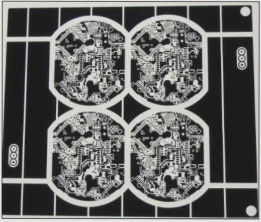
In PCB production, film is used to create precise images of circuit patterns. These films are typically made of high-quality photographic materials and serve as a template for transferring circuit designs onto the copper layers of the PCB. The process involves placing the film over the board and exposing it to light, where areas corresponding to the circuit patterns are hardened. The unexposed areas are then removed, leaving behind the circuit layout that will guide the etching process.
In summary, when discussing “film” in the context of PCBs, we are referring to the photographic negatives used for pattern transfer during the board manufacturing process.
### Film Processing for PCB Production: A Detailed Overview
In the PCB (Printed Circuit Board) production process, films are essential for creating the design on the board. These films are typically black, with an English symbol or number indicating the specific film type. In the corner of each film, the color—C, M, Y, or K (Cyan, Magenta, Yellow, or Black)—is marked to indicate the color output. The color is determined by the angle of the screen if it’s not directly labeled. Alongside the film, a stepped color bar is used for dot density calibration, ensuring proper dot formation.
#### Color Bar and Dot Density Calibration
The color bar serves not only to check dot density but also to identify the CMYK components. The placement of the color bar indicates its color: C is in the lower-left corner, M in the upper-left, Y in the upper-right, and K in the lower-right. This system helps the printing factory quickly identify the CMYK components, streamlining the quality control process. Additionally, the number of colors to be printed is determined by the screen line for each film, which ensures the correct balance of colors and clarity in the final print.
#### Structure and Composition of the Film
The film consists of several layers: a protective film, emulsion layer, bonding film, film base, and anti-halation layer. Key materials in the emulsion layer include silver salt photosensitive material, gelatin, and pigments. The silver salts react to light and reduce to silver particles, while gelatin suspends these particles to allow coating onto the film base. The emulsion is sensitized with pigments, and exposure to light results in the creation of a latent image on the film.
#### Film Processing Steps
The processing of the film follows several key stages: exposure, development, fixing, washing, and air-drying. The precise handling of each step is crucial to achieving a high-quality result.
1. **Exposure and Latent Image Formation**
– When the film is exposed to light, the silver salts in the emulsion form a latent image. At this stage, no visible graphic is yet present. This process is essential for transferring the circuit design onto the film.
2. **Development**
– During development, the exposed silver salts are reduced to black silver particles. Manual development requires the film to be evenly immersed in the developer solution. The silver salt film used in PCB production typically has a low photosensitive speed, allowing the process to be conducted under a safety light. It’s important that the light is not too bright to avoid damage to the negative film. Development is complete when the black images on the film, both front and back, have consistent color depth. The developer temperature should be maintained between 18°C and 25°C to ensure optimal processing speed.
– **Machine Development**: For automatic development, the concentration of the developer solution typically follows a 1:4 ratio, with one part developer to four parts water.
3. **Fixing**
– After development, the film undergoes a fixing process to remove any unexposed silver salts. This ensures that only the desired image remains on the film. The fixing solution dissolves the unexposed silver salts, preventing them from affecting the final image. The fixing time should be sufficient to make the film transparent where no photosensitive material is present.
– **Machine Fixing**: Similar to the development process, fixing can be automated using a film processing machine. The concentration of the fixing solution can be slightly thicker than that of the developer solution to ensure thorough fixing.
4. **Washing**
– The fixed film contains chemicals like sodium thiosulfate, which must be washed off to prevent the film from turning yellow or becoming invalid. The film should be rinsed with running water for at least 15 to 20 minutes. For machine processing, this step is automated and ensures the film is thoroughly cleaned.
5. **Air-Drying**
– Once the washing is complete, the film should be air-dried in a cool, dry environment. Proper air-drying prevents any moisture from remaining on the film, which could affect its clarity and quality.
#### Key Considerations in Film Processing
– **Avoid Scratching the Film**: Throughout the processing stages, care must be taken not to scratch the film surface, as any damage can affect the quality of the final print.
– **Chemical Safety**: It is crucial to handle chemicals, such as developers and fixers, with care. Direct contact with the skin or clothing should be avoided to prevent burns or staining.
#### PCB Tin Plating Challenges
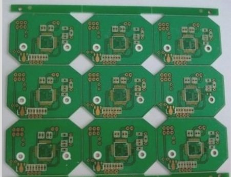
One of the major challenges in PCB production is poor tinning, which can lead to several issues such as circuit sand holes, chipping, open circuits, and issues with copper coverage in drilled holes. If the tin is not properly cleaned or if multiple returns of the tinning process occur, these issues can become exacerbated. Poor tinning often results in the need to redo the soldering process or even scrap the entire PCB design, leading to significant delays and added costs.
In conclusion, the process of developing and processing film for PCB production requires careful attention to detail at every stage. From exposing the film to the final air-drying process, maintaining precise conditions ensures the quality and integrity of the final printed circuit board. Additionally, proper tinning practices are crucial to avoid costly production setbacks.
**Reasons for Poor Tinning on PCB Boards**
Poor tinning on PCB boards during the SMT (Surface Mount Technology) production process can occur for several reasons, most of which are related to the preparation and conditions during the tinning process. The primary factors contributing to poor tinning include:
1. **Surface Contamination**: The cleanliness of the bare PCB surface is crucial for proper tinning. Any contaminants such as dust, oil, or oxidation can prevent the solder from adhering effectively, leading to poor tinning. It is essential to ensure that the PCB surface is thoroughly cleaned before the tinning process.
2. **Inadequate Flux**: The flux used during tinning plays a vital role in ensuring proper solder adhesion. If the flux is of poor quality or not applied in sufficient quantity, it can result in poor wetting of the solder, leading to incomplete or uneven tinning.
3. **Improper Temperature**: Temperature control is critical during the tinning process. If the soldering temperature is too low, the tin may not melt or spread evenly across the PCB surface. Conversely, if the temperature is too high, it may cause excessive oxidation or damage to the PCB, both of which contribute to poor tinning.
4. **Insufficient Solder Contact**: In some cases, improper contact between the PCB and the solder can lead to poor tinning. This may be caused by insufficient solder volume or poor mechanical alignment during the soldering process.
In conclusion, poor tinning on PCB boards is typically the result of inadequate surface preparation, improper flux use, or incorrect temperature settings during the tinning process. Ensuring that these factors are properly controlled is crucial for achieving high-quality tinning results.