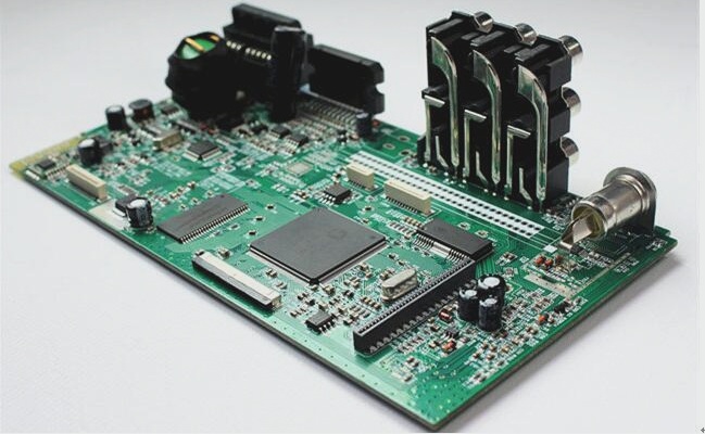
Introduction:
With the continuous expansion of flexible printed circuit boards (FPC) across various applications, FPC products are expected to evolve similarly to rigid printed circuit boards (PCBs). The variety, types, structures, and grades of FPCs will see rapid growth and diversification, driven by both domestic and international market trends.
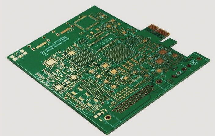
Flex-PCB Manufacturing Process:
Common manufacturing processes for double-sided and multilayer flexible PCBs include the following:

Materials Preparation (Blanking):
The material preparation for Flex-PCB mainly includes flexible copper-clad laminates, cladding layers, and reinforcement plates. The primary auxiliary materials used during lamination include separation films, conformal materials or silicone rubber sheets, ink-absorbing or coated papers, among others.
Drilling:
Flexible copper-clad laminates and cladding layers are soft and thin, making them difficult to drill. As a result, stacking is required before drilling, meaning multiple layers of cladding or copper-clad laminates are stacked together like a book.
Desmear and Pitting:
After drilling, resin debris on the walls of PCB holes must be completely removed to ensure high-quality plated-through holes (PTH). Typically, desmearing and pitting processes are required before conducting PTH.
- PTH and Pattern Plating:

- Electroless Plating:
The pre-treatment solution should ideally use acidic colloidal palladium rather than alkaline ionic palladium. Proper control of reaction time and speed is crucial to avoid damaging the flexible materials and compromising the copper layer’s mechanical properties.
- Electrical Plating:
Electroless copper plating layers have poor mechanical properties (e.g., ductility), making them susceptible to breaking under thermal shock. Therefore, once the chemical copper plating layer reaches 0.3–0.5 microns, electrical plating should be performed to thicken the copper layer to 3–4 microns and ensure the integrity of hole wall coatings.
- Pre-cleaning and Imaging:
Prior to imaging, the PCB surface must be cleaned and roughened. This process is similar to that of rigid PCBs. However, since flexible substrates are prone to deformation and bending, chemical or electrolytic cleaning is recommended. The process of applying dry film, exposure, and development is analogous to that of rigid PCBs. After development, the dry film becomes brittle and may lose its adhesion to the copper foil, so extra care must be taken to prevent warping or peeling.
Etching:
Flexible substrates often contain long parallel traces that require consistent etching. To ensure uniform etching, attention should be paid to the spraying direction, pressure, position, and transmission direction of the etching solution. It is also recommended to use a rigid substrate in front of the flexible substrate during etching to assist in forward movement. Additionally, an automatic regeneration system for etching fluid is preferred.
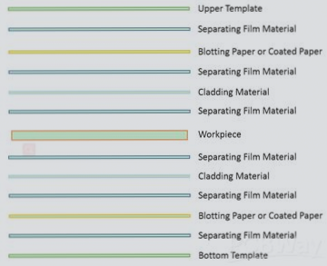
Position of Cladding Layer:
After etching, PCBs need surface treatment to enhance adhesion before applying the cladding layer. Due to moisture absorption, both the drilled cladding layer and the etched flexible PCBs must be dried in an oven for 24 hours before lamination. The stack-up height should not exceed 25mm.
Lamination:
- Lamination of Cladding Layer for Flex-PCB:
The lamination process for flexible PCBs depends on the specific substrate material, and includes controlling the lamination time, heating rate, and pressure. The following process parameters are typically used:
1. Lamination Time: The net pressure time under full pressure is 60 minutes.
2. Heating Rate: The temperature should reach 173°C within 10 to 20 minutes from the ambient temperature.
3. Pressure: Apply a pressure of 150N-300N/cm², reaching full pressure within 5-8 seconds.
2) Gasket Material for Lamination:
The selection of gasket material is crucial for the lamination quality of flexible and rigid-flex PCBs. The ideal gasket material should have excellent formability, low fluidity, and minimal shrinkage during the cooling process, ensuring no bubbles or deformation during lamination. Gasket materials are generally classified into flexible and rigid systems. The flexible system primarily includes PVC film or radiation-crosslinked polyethylene films, along with other thermoplastic materials. The rigid system is mainly composed of glass cloth reinforced with silicone rubber.
Baking: The main purpose of baking is to remove moisture from the PCB during processing.
HASL or Hot Melting: After drying, the PCB should undergo HASL (Hot Air Solder Leveling) or hot melting immediately to prevent moisture absorption.
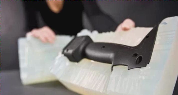
Sharp Processing: The shaping of flexible PCBs is carried out using seamless, precision steel dies in mass production. These dies can be designed as single-cavity molds or multi-cavity molds.
Packaging & Shipping: Flexible PCBs should not only be separated using wrapping paper or foam pads. For better protection, multiple boards are often stacked with foam pads and vacuum-sealed using a vacuum packaging machine. Alternatively, vacuum bags with desiccants can be used to extend storage life. Wellcircuits provides flexible shipping options for our customers. You can choose from services such as FedEx, DHL, EMS, UPS, TNT, Hong Kong Post, and more.
If you have any questions about PCBs or PCBA, please contact us at info@wellcircuits.com.