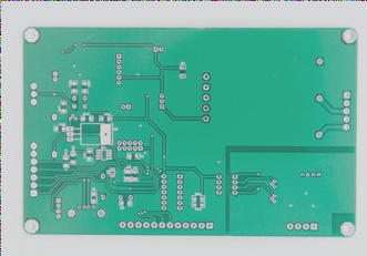
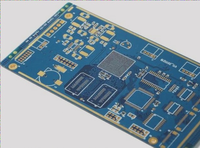
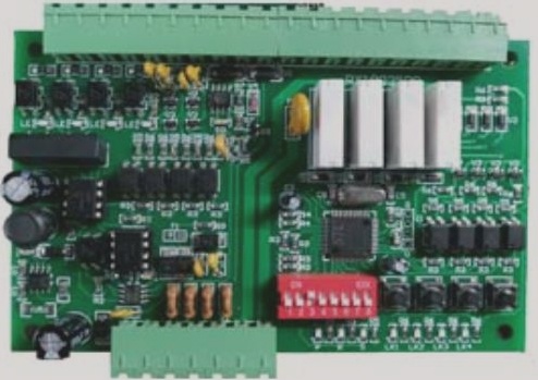
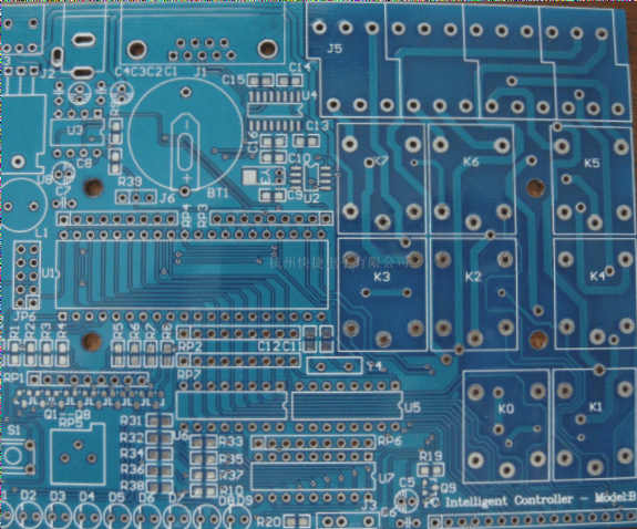
PCB Design Guidelines
One. Line Specifications
- Minimum Line Width: 6 mil (0.153 mm)
- Minimum Line Spacing: 6 mil (0.153 mm)
- Distance Between Line and Outline: 0.508 mm (20 mil)
In PCB manufacturing, it is crucial to adhere to specific line width and spacing requirements. A wider line width, preferably around 10 mil, can enhance factory yield and is considered optimal for design.
Two. Via (Conductive Hole) Requirements
- Minimum Aperture: 0.3 mm (12 mil)
- Minimum Pad Size: 6 mil (0.153 mm)
- Minimum Spacing Between Via Holes: 6 mil
- Distance Between Pad and Outline: 0.508 mm (20 mil)
Proper via specifications, including minimum aperture and spacing, are essential for successful PCB design and production.
Three. PAD (Plug-in Hole) Guidelines
- Minimum Plug-in Hole Size: Component pin size + 0.2mm
- Outer Ring Size: Not less than 0.2mm (8 mil)
- Minimum Hole-to-Hole Spacing: 0.3mm
- Distance Between PCB Pad and Outline Line: 0.508mm (20 mil)
Adhering to proper pad specifications ensures smooth component insertion and overall circuit board functionality.
Four. Solder Mask and Character Design
- Solder Mask Window: Minimum 0.1mm (4 mil) for SMD
- Character Width: Minimum 0.153mm (6 mil)
- Character Height: Minimum 0.811mm (32 mil)
Clear and precise character design is crucial for effective PCB production and assembly.
Five. Additional Considerations
- Non-Metalized Slotted Holes: Minimum spacing of 1.6mm
- PCB Imposition: No gaps, minimum gap size of 1.6mm
Ensuring proper specifications for non-metalized holes and PCB imposition is essential for successful circuit board manufacturing.