Introduction to SMT Patch Factory Production Process
The technical team at the solution company frequently collaborates with SMT patch production factories. However, for those who haven’t visited the factory in person, understanding the fundamental production process and key procedures might be challenging. To facilitate comprehension for relevant individuals, here’s an overview of the basic process and important procedures involved:
Basic Process of SMT Patch Factory
- Incoming Inspection: Initial inspection of components.
- Burning: Process of burning components onto the PCB.
- Printing: Application of solder paste onto the PCB.
- Inspection: Quality check post-printing.
- Placement: Mounting components onto the PCB.
- Pre-furnace Inspection: Pre-soldering quality check.
- Reflow Soldering: Solder paste melting process.
- AOI Inspection: Automated Optical Inspection for quality assurance.
- Repair: Rectification of any defects.
- Test: Testing the assembled PCB.
- Assembly: Final assembly of the product.
Key Procedures in SMT Patch Processing
Despite the complexity, printing, patching, and reflow soldering are the three essential processes in SMT patch processing. These processes have remained unchanged for the past decade and are now fully automated.
SMT Patch Printing
SMT patch printing involves applying solder paste onto the PCB using specialized equipment. The key components for printing include:

- Printing Machine: Fully automatic or semi-automatic machines used for printing.
- Solder Paste: Material used to secure components to the PCB.
- Stencil: Mold outlining pad positions on the PCB for solder paste application.
Printing Process
The printing process involves stencil installation, solder paste application, and PCB feeding through the machine. The machine aligns the PCB and stencil, presses them together, and transfers solder paste onto the PCB pads through the stencil’s openings. This step is critical, with 70% of SMT process defects attributed to this stage.
SMT Placement Process
SMT placement, or mounting, involves placing components onto the PCB using advanced equipment. The process has evolved from manual soldering to automated systems, enhancing production efficiency.
Placement Machine Operation
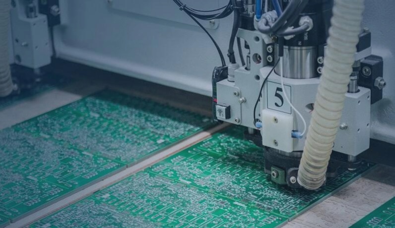
To operate a placement machine, customer-provided files are used to create the placement program. The machine utilizes a placement head, feeder, and track to accurately mount components onto the PCB.
SMT Patch Processing Overview
-
Suction Nozzle
The placement head is equipped with 12 suction nozzles that use vacuum to pick up components.
-
Feeder System
The feeder system is set up based on the placement program. Materials are installed on the feeders according to a station table and then arranged on the placement machine. The gear drives the material tape, advancing it as per the program instructions, allowing the suction nozzle to pick and place components at specified coordinates.
-
Reflow Soldering
After solder paste printing and component placement, the PCB undergoes manual inspection or AOI (Automated Optical Inspection) before entering the reflow oven. Reflow soldering involves the solder paste melting and solidifying to form solder joints. The reflow oven, a rectangular chamber with a chain conveyor, heats the PCB using a hot air system divided into multiple temperature zones:
-
Preheating Zone
This zone heats the PCB and components to achieve thermal equilibrium and initiate solder paste movement.
-
Constant Temperature Zone
Removes surface oxides and activates the solder paste.
-
Reflow Area
The highest temperature area where solder paste melts. Lead-free solder paste typically melts at around 220°C, taking about 40 seconds.
-
Cooling Zone
Gradually cools the PCB to solidify the solder joints.
- The entire reflow process typically lasts about 6 minutes, encompassing the essential SMT processes of printing, placing, and reflow soldering.


