Hi all,
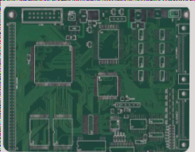
I was just cracking open a cheap USB current meter and found something I can’t really explain. The main micro in a TQFP package has several pins covered in soldermask AND silkscreen (see attachment). Is there any reason why one would do that instead of just leaving out these pins on the solder stencil and/or just solder them to pads that aren’t connected to any net?
I always solder n/c pins to unconnected pads just for the sake of the added mechanical stability. The only possible reason I can think of why they are not just left out from the solder paste stencil is to make sure they are also not connected when wave soldering or to make sure these pads don’t “thieve” the solder from the surrounding pads, but this leaves the question of why not soldering them in the first place and the only explanation I can think of for this would be cost, but can this really be a reason? I think we’re talking femto-cents/unit here
Also: Why silkscreening instead of just solder-masking the pads? Visual indication of which pads are unconnected?
Thanks for any insights
Daniel
Edit: I just noticed that there are actually traces going under / to these pads. In case they go under these pads it may be to make space to easily route these traces?


