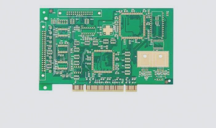
Via Holes in PCB Boards
Via holes play a crucial role in multi-layer PCB boards, with drilling costs typically making up a significant portion of production expenses. Essentially, each hole on a PCB serves as a via. Vias serve two primary functions: facilitating electrical connections between layers and providing support for device fixation or positioning. They are categorized as blind vias, buried vias, and through vias based on their location and purpose.
Types of Vias
- Blind Vias: Connect the surface circuit to the underlying inner circuit with limited depth.
- Buried Vias: Located within the inner layers of the PCB, these vias do not extend to the board’s surface.
- Through Vias: Penetrate the entire PCB and can be used for internal connections or component mounting.
Designers focus on optimizing via size, consisting of the middle hole and the surrounding pad area. Smaller vias are preferred in high-speed and high-density PCB designs to maximize wiring space and reduce parasitic capacitance, benefiting high-speed circuits.
Considerations for Via Design
While smaller vias offer advantages, such as reduced parasitic capacitance, shrinking their size increases production costs. Factors like drilling and electroplating limitations restrict how small vias can be made. For instance, the depth-to-diameter ratio affects copper plating uniformity. Balancing size and functionality is crucial in PCB design.
Parasitic Capacitance Effects
Via holes inherently possess parasitic capacitance to the ground, impacting signal rise time and circuit speed. Understanding the relationship between via dimensions, board thickness, and dielectric constants helps estimate parasitic capacitance effects. Designers must account for these factors, especially in multi-layer PCBs.
Parasitic Inductance Concerns
Alongside parasitic capacitance, vias exhibit parasitic inductance that can significantly impact high-speed digital circuit performance. The series inductance of vias may compromise bypass capacitor efficiency and diminish the overall power system filtering capabilities. Addressing parasitic inductance is vital in optimizing PCB designs for high-speed applications.
The Impact of Via Design on High-Speed PCB Boards
When designing high-speed PCB boards, it is crucial to consider the impact of via design on circuit performance. The diameter of the via has minimal effect on inductance, while the length of the via significantly affects inductance. For example, the inductance of a via can be calculated using the formula L=5.08×0.050[ln(4×0.050/0.010) 1]=1.015nH. If the signal has a rise time of 1ns, the equivalent impedance is XL=πL/T10-90=3.19Ω. This impedance becomes significant when high-frequency currents pass through.
Key Considerations for Via Design:
- Choose a via size that balances cost and signal quality. For instance, for a 6-10 layer memory module PCB board design, consider using 10/20Mil (drilling/pad) vias. Smaller vias are challenging to implement under current technical constraints. For power or ground vias, opt for larger sizes to reduce impedance.
- Thinner PCB boards help reduce parasitic parameters of vias.
- Minimize unnecessary vias to avoid changing signal trace layers.
- Drill power supply and ground pins close together to minimize lead length and inductance. Use thick leads for power and ground to reduce impedance.
- Place grounded vias near signal layer changes to provide a close return path. Consider adding redundant ground vias on the board for better performance.
In high-density via scenarios, adjusting via positions and reducing pad sizes can help prevent circuit breaker formation on copper layers. Flexibility in design is essential to optimize via performance.

