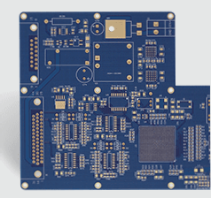
Understanding PCB and PCBA in Electronics Manufacturing
PCB, or Printed Circuit Board, is a vital component in the electronics industry. It provides support for electronic parts and enables their electrical connections. PCBs are known for their:
- High wiring density, compact size, and lightweight nature, contributing to device miniaturization.
- Consistency in graphics and wiring, reducing errors and maintenance time.
- Facilitation of mechanization and automated production, enhancing productivity.
- Standardized designs for easy interchangeability.
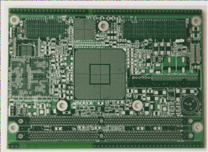
The Role of PCBA in Electronics Assembly
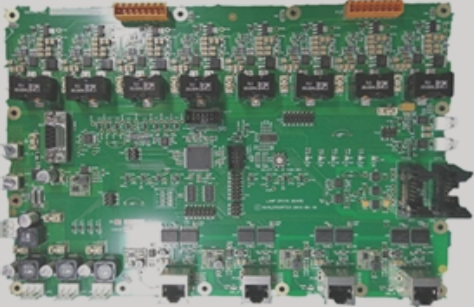
PCBA, or Printed Circuit Board Assembly, involves the complete manufacturing process of PCBs, including Surface Mounted Technology (SMT) and Dual In-line Package (DIP) insertion methods.
SMT utilizes mounters for placing small components on PCBs, while DIP involves inserting larger components into pre-drilled holes. The primary processes for SMT and DIP are:
- SMT: PCB positioning, solder paste printing, component mounting, reflow oven passing, and final inspection.
- DIP: Adhesive application, component insertion, wave soldering, and inspection.
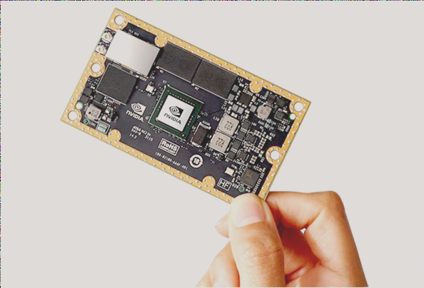
Distinguishing PCB from PCBA
PCBA signifies a completed circuit board after all manufacturing processes, while PCB refers to a bare board without components. In essence, PCBA is a finished board, whereas PCB is unpopulated.
COB Requirements for PCB Design
COB (Chip on Board) necessitates PCBs due to the absence of a lead frame for IC packaging. For COB designs, the PCB pad must use electroplated gold or ENIG finishes to ensure connectivity. Key considerations include:
- Thicker electroplated gold or ENIG layers for Die Bonding energy.
- Consistent solder wire lengths in the wiring area to prevent short circuits.
Essential Tips for PCB Design
- When designing a COB wafer, it is advisable to have a minimum of two positioning points. Opt for cross-shaped points over circular ones to align better with Wire Bonding machines.
- Ensure that the Die Pad size on the PCB is slightly larger than the wafer to minimize placement errors and prevent wafer rotation. The pads should be 0.25 to 0.3 mm larger on each side.
- Avoid placing via holes in areas where glue is needed for COB. If unavoidable, make sure the manufacturer seals these holes completely to avoid epoxy leakage into the PCB.
If you require PCB manufacturing services, feel free to contact us.