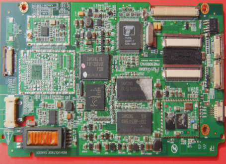
1. Grind the chip using fine sandpaper to remove the model number on the PCB chip. This method is particularly effective for chips with a side door.
2. Seal with adhesive that solidifies into a solid, covering both the PCB and its components. Intentionally twist together five or six flying wires (preferably thin enameled wire) to complicate removal without breaking the flying lines. Avoid corrosive adhesives; minimal heat should be generated in the enclosed area.
3. Employ a dedicated encryption chip.

4. Use a chip that cannot be cracked; however, this option comes with a cost.
5. Use MASKIC; generally speaking, MASKIC is much harder to crack than a programmable chip. MASK (mask): MCU mask means that the program data has been converted into lithographic version during single-chip production. The key advantage is reliable programming at a low cost. Disadvantages include large batch requirements, needing lithography remade for every program modification, inability to produce different programs simultaneously, and extended delivery cycles.
6. Utilize bare chips to conceal the chip model and obscure wiring from potential thieves. However, ensure the chip’s function is not easily deducible; it’s advantageous to mix it with other components like small ICs and resistors.
7. Series-connect a resistance of 60 ohms or more on low-current signal lines to prevent multimeter audible on-off indications.
8. Incorporate more small components without labels or with minimal coding in signal processing, such as small chip capacitors.
9. Cross certain address and data lines (excluding RAM) that are reverted in software to enhance security.
10. Implement PCBs with buried and blind hole technology to conceal vias within the board, albeit at higher costs suitable only for products, thereby raising the replication difficulty.
Analysis of Traditional PCB Design Methods:
Traditional PCB design follows a sequential process of schematic design, layout design, PCB production, and subsequent testing and debugging.
During the schematic design phase, due to the absence of effective analysis tools, designers must pre-analyze signal transmission characteristics on actual PCBs. Typically, schematic designs rely on component data manuals or previous design experiences. For new projects, selecting correct component parameters, circuit topologies, and network terminations can be challenging.
In PCB layout design, real-time analysis and evaluation tools are lacking for assessing laminate planning, component placement, and wiring impacts. Therefore, the quality of layout design heavily depends on designer experience.
In the traditional PCB design process, final PCB performance evaluation occurs post-production. If performance criteria aren’t met, extensive testing is required, particularly for schematic and layout design parameters that are difficult to quantify, necessitating iterative adjustments. As systems grow more complex and design cycles shorten, improving PCB design methods and processes becomes essential to meet modern high-speed system requirements.
2. Seal with adhesive that solidifies into a solid, covering both the PCB and its components. Intentionally twist together five or six flying wires (preferably thin enameled wire) to complicate removal without breaking the flying lines. Avoid corrosive adhesives; minimal heat should be generated in the enclosed area.
3. Employ a dedicated encryption chip.

4. Use a chip that cannot be cracked; however, this option comes with a cost.
5. Use MASKIC; generally speaking, MASKIC is much harder to crack than a programmable chip. MASK (mask): MCU mask means that the program data has been converted into lithographic version during single-chip production. The key advantage is reliable programming at a low cost. Disadvantages include large batch requirements, needing lithography remade for every program modification, inability to produce different programs simultaneously, and extended delivery cycles.
6. Utilize bare chips to conceal the chip model and obscure wiring from potential thieves. However, ensure the chip’s function is not easily deducible; it’s advantageous to mix it with other components like small ICs and resistors.
7. Series-connect a resistance of 60 ohms or more on low-current signal lines to prevent multimeter audible on-off indications.
8. Incorporate more small components without labels or with minimal coding in signal processing, such as small chip capacitors.
9. Cross certain address and data lines (excluding RAM) that are reverted in software to enhance security.
10. Implement PCBs with buried and blind hole technology to conceal vias within the board, albeit at higher costs suitable only for products, thereby raising the replication difficulty.
Analysis of Traditional PCB Design Methods:
Traditional PCB design follows a sequential process of schematic design, layout design, PCB production, and subsequent testing and debugging.
During the schematic design phase, due to the absence of effective analysis tools, designers must pre-analyze signal transmission characteristics on actual PCBs. Typically, schematic designs rely on component data manuals or previous design experiences. For new projects, selecting correct component parameters, circuit topologies, and network terminations can be challenging.
In PCB layout design, real-time analysis and evaluation tools are lacking for assessing laminate planning, component placement, and wiring impacts. Therefore, the quality of layout design heavily depends on designer experience.
In the traditional PCB design process, final PCB performance evaluation occurs post-production. If performance criteria aren’t met, extensive testing is required, particularly for schematic and layout design parameters that are difficult to quantify, necessitating iterative adjustments. As systems grow more complex and design cycles shorten, improving PCB design methods and processes becomes essential to meet modern high-speed system requirements.


