PCB assembly is the process of integrating a circuit board with other electronic components such as connectors, housings, and heat sinks to form a finished product.
1. PCB Assembly Design: Considering PCB assembly during the initial design phase is crucial for achieving an optimal product. A common issue among beginners is designing the board without considering the assembly process. They often focus solely on the PCB itself without understanding manufacturing challenges.
2. While the PCB design may appear functional on its own, significant assembly errors can arise later. For instance, components placed too closely together can lead to operational failures or performance issues in the final product. Component availability is another critical factor; delays can occur if necessary components are not readily accessible. How can these issues be mitigated?
3. Proper spacing between components is essential to prevent interference and ensure smooth assembly. Components placed too closely may require redesign and manufacturing adjustments, resulting in costly delays. Maintaining adequate gaps between component boundaries helps minimize these risks.
4. When positioning components, it’s crucial to avoid overlap in their shapes. Generally, routing and layout guidelines recommend a minimum spacing of 10 mils for discrete components like capacitors and resistors, with 30 mils being preferred. Additional spacing rules should also be observed, as outlined below.
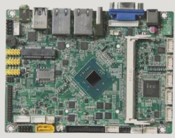
This helps ensure minimal conflict between design and actual assembly. Smaller components occupy less PCB space, so assess if reducing their size can create additional PCB space.
Lead-free components should not be mixed with those containing lead. If lead-free assembly is required and standard lead adhesive isn’t available, the entire PCB, including components, must be assembled lead-free.
Sometimes, a specific device may only offer a lead-free BGA package with specific requirements. Poor coordination between PCB fabrication and assembly can leave separating pieces between PCBs after wiring, hindering connector assembly extending to that edge.
Distribute large components evenly on the PCB during layout to achieve better heat distribution during reflow. Ensure the PCB vendor has a reflow profile appropriate for the reflow amount.
Minimize technique mixing. Place plug-ins on the same board side to reduce PCB manufacturing and assembly costs and time.
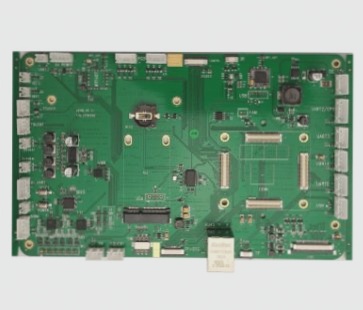
Mechanical drilling, such as 6 mil, is very small and not recommended unless absolutely necessary due to BGA density. A pad size of 18.5 mil and drilling of 8 mil (18.5/8) is recommended. Ideally, 22/10 would be acceptable, but it is not feasible with BGAs.
Components used in the design should be double-checked early in the layout process. If there is extra board space and unnecessary larger widgets are used in the current design, designers should consider recommending larger components. This approach helps streamline the assembly process, avoiding multiple steps. For instance, opting for 0805 resistors instead of 1206 where possible reduces PCB size and complexity.
Component availability can cause significant delays. Therefore, it’s crucial to check inventory, delivery schedules, and component discontinuations during the design phase.
The bill of materials (BOM) is critical for design and assembly. Issues in the BOM can halt the PCB fabrication process until resolved by engineers. To keep the BOM current, it should be reviewed whenever there are design changes.
When adding new components to the schematic during layout, ensure the BOM is updated with accurate part numbers, descriptions, and assembly specifications. Engineers may change components during the design phase due to lead times, size constraints, or availability, often forgetting to update the BOM with the new part numbers. This oversight can lead to assembly problems and delays.

Nowadays, many PCB factories offer one-stop services encompassing PCB board design, material procurement, stencil fixtures, and PCB assembly. However, if your components are not all supplied by the PCB manufacturer, you must organize and provide them in a kit that aligns precisely with the BOM (Bill of Materials). SMT components must be provided in rolls, continuous tapes of at least 6 inches in length, or in tubes or trays.
Another critical aspect of layout design is the component footprint. It is crucial to accurately utilize the footprint dimensions specified in the datasheet to ensure the correct placement of parts and pad patterns. Misinterpreting the datasheet can lead to incorrect footprints, necessitating complete PCB redesign and remanufacturing.
Each component connection must have its own dedicated pad, each sized appropriately to match its corresponding mating piece. Sharing a single pad between two components, such as a resistor and a capacitor, will result in improper alignment during assembly.
1. One important way to ensure that your PCB is error-free and works seamlessly is to conduct design for manufacturing (DFM) tests.
2. These tests identify most errors in the design at an early stage, thus avoiding costly errors and delays later on.
3. Issues such as spacing, component polarity, and package verification can be identified promptly and addressed.
1. PCB Assembly Design: Considering PCB assembly during the initial design phase is crucial for achieving an optimal product. A common issue among beginners is designing the board without considering the assembly process. They often focus solely on the PCB itself without understanding manufacturing challenges.
2. While the PCB design may appear functional on its own, significant assembly errors can arise later. For instance, components placed too closely together can lead to operational failures or performance issues in the final product. Component availability is another critical factor; delays can occur if necessary components are not readily accessible. How can these issues be mitigated?
3. Proper spacing between components is essential to prevent interference and ensure smooth assembly. Components placed too closely may require redesign and manufacturing adjustments, resulting in costly delays. Maintaining adequate gaps between component boundaries helps minimize these risks.
4. When positioning components, it’s crucial to avoid overlap in their shapes. Generally, routing and layout guidelines recommend a minimum spacing of 10 mils for discrete components like capacitors and resistors, with 30 mils being preferred. Additional spacing rules should also be observed, as outlined below.

This helps ensure minimal conflict between design and actual assembly. Smaller components occupy less PCB space, so assess if reducing their size can create additional PCB space.
Lead-free components should not be mixed with those containing lead. If lead-free assembly is required and standard lead adhesive isn’t available, the entire PCB, including components, must be assembled lead-free.
Sometimes, a specific device may only offer a lead-free BGA package with specific requirements. Poor coordination between PCB fabrication and assembly can leave separating pieces between PCBs after wiring, hindering connector assembly extending to that edge.
Distribute large components evenly on the PCB during layout to achieve better heat distribution during reflow. Ensure the PCB vendor has a reflow profile appropriate for the reflow amount.
Minimize technique mixing. Place plug-ins on the same board side to reduce PCB manufacturing and assembly costs and time.

Mechanical drilling, such as 6 mil, is very small and not recommended unless absolutely necessary due to BGA density. A pad size of 18.5 mil and drilling of 8 mil (18.5/8) is recommended. Ideally, 22/10 would be acceptable, but it is not feasible with BGAs.
Components used in the design should be double-checked early in the layout process. If there is extra board space and unnecessary larger widgets are used in the current design, designers should consider recommending larger components. This approach helps streamline the assembly process, avoiding multiple steps. For instance, opting for 0805 resistors instead of 1206 where possible reduces PCB size and complexity.
Component availability can cause significant delays. Therefore, it’s crucial to check inventory, delivery schedules, and component discontinuations during the design phase.
The bill of materials (BOM) is critical for design and assembly. Issues in the BOM can halt the PCB fabrication process until resolved by engineers. To keep the BOM current, it should be reviewed whenever there are design changes.
When adding new components to the schematic during layout, ensure the BOM is updated with accurate part numbers, descriptions, and assembly specifications. Engineers may change components during the design phase due to lead times, size constraints, or availability, often forgetting to update the BOM with the new part numbers. This oversight can lead to assembly problems and delays.

Nowadays, many PCB factories offer one-stop services encompassing PCB board design, material procurement, stencil fixtures, and PCB assembly. However, if your components are not all supplied by the PCB manufacturer, you must organize and provide them in a kit that aligns precisely with the BOM (Bill of Materials). SMT components must be provided in rolls, continuous tapes of at least 6 inches in length, or in tubes or trays.
Another critical aspect of layout design is the component footprint. It is crucial to accurately utilize the footprint dimensions specified in the datasheet to ensure the correct placement of parts and pad patterns. Misinterpreting the datasheet can lead to incorrect footprints, necessitating complete PCB redesign and remanufacturing.
Each component connection must have its own dedicated pad, each sized appropriately to match its corresponding mating piece. Sharing a single pad between two components, such as a resistor and a capacitor, will result in improper alignment during assembly.

1. One important way to ensure that your PCB is error-free and works seamlessly is to conduct design for manufacturing (DFM) tests.
2. These tests identify most errors in the design at an early stage, thus avoiding costly errors and delays later on.
3. Issues such as spacing, component polarity, and package verification can be identified promptly and addressed.

 العربية
 简体中文
简体中文 Nederlands
 English
 Français
 Deutsch
 Italiano
 日本語
日本語 한국어
한국어 Português
 Русский
 Español
 ไทย
ไทย