Surface Mount Assembly Process
Initially, all PCBs were assembled by hand using a soldering iron. However, as technology advanced, components became smaller and more challenging to assemble manually. Additionally, the number of components that could fit onto a single board increased, creating the need for automated assembly processes.

Required Elements
Below are the essential files and data required for automated assembly:
-
Gerber files in 274-X format (including embedded apertures) with the fabrication drawing.
-
Part centroid text file, including Reference Designators, external placement layer, and X & Y coordinates with rotation in ASCII format.
-
Numerical Control (NC) drill files.
-
Solder paste file (one of the Gerber files) for all mounted sides.
-
Glue dot file.
-
Design database, if possible, specifying the format (program name).
-
Bill of Materials (BOM), detailing the components required for assembly.
-
List of parts or hardware required for assembly.
The Gerber files are essential for defining pad locations on the PCB, helping the assembly house determine the position of components, and providing a visual reference of the board layout. The database can also be used to locate pin 1 of each component. Some assembly houses may generate their own solder paste files or stencils. Designers can also create the solder paste file based on their preferences and experience. It’s beneficial to understand how assembly houses create stencils to maintain consistency in the process across different manufacturers.
The solder paste file is used to mask the entire board, leaving only the areas where soldering is required. Solder paste is applied to these exposed pads, and then the stencil is removed. Components are then placed onto the board and held in place by the paste, with glue dots used to secure them until the soldering process is complete.
For proper component placement, a centroid file is required to identify the center of each part. The placement layer indicates which side of the PCB the component will be mounted on, while the rotation field shows the component’s orientation.
Consistent component orientation is critical for accurate assembly. Unless the designer’s software can automatically adjust for discrepancies, all components should be positioned in the same orientation.
NC drill files define the locations and sizes of mounting holes, providing the necessary dimensions for through-hole components. These files also ensure that there’s sufficient clearance for component leads during assembly.
The Bill of Materials (BOM) is used to correlate the component designators from the centroid file with the actual components required for assembly. The BOM should also specify whether each component is a surface-mount (SM) or through-hole component.

Other Considerations
Other considerations for automated assembly include board size, panel size, and breakaways. Typically, the boards are assembled on a panel that may contain multiple boards. The panel is the original material from which the boards are etched and routed. These panels are sent to the assembly house with all boards intact.
Note: Breakaways refer to the connections around each board that hold it in place during assembly. These connections can be easily broken when it’s time to remove the board.
1. Ordering a Board
Wellcircuits offers a one-stop solution for PCB and prototype assembly.
2. DFM Check
The Design for Manufacturability (DFM) check reviews all the design specifications of a PCB. It ensures that no design elements are missing, redundant, or potentially problematic. These issues, if left unchecked, could severely impact the functionality of the final product. For instance, one common flaw in PCB designs is insufficient spacing between components, which could lead to short circuits or other malfunctions.
By identifying potential issues before manufacturing begins, DFM checks can significantly reduce manufacturing costs and minimize unforeseen expenses by preventing the need to scrap faulty boards.

3. Incoming Quality Control (IQC)
Wellcircuits verifies all incoming materials and addresses any quality issues before proceeding with SMT (Surface Mount Technology) assembly. Our IQC team inspects the following aspects to ensure that materials meet our strict standards:
- Model number and quantities according to the BOM (Bill of Materials) list
- Physical condition (e.g., deformation, broken pins, oxidation), especially for ICs and complex components
- Sample testing of incoming materials using tools like a test frame and multimeter
- If any defects or discrepancies are found, the materials are returned to the supplier or customer
4. Machine Programming – Gerber/CAD to Centroid/Placement/XY File
Once the PCB panels and components are received, the next step is to set up the machines used in the manufacturing process. Equipment such as placement machines and Automated Optical Inspection (AOI) systems require programming, typically generated from CAD data. However, if CAD data is unavailable, Gerber data—required for the bare PCB production—is used as a substitute.
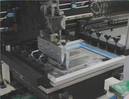
5. Solder Paste Printing
The first machine to be set up in the manufacturing process is the solder paste printer. This machine applies solder paste to the appropriate pads on the PCB using a stencil and squeegees.
6. Component Placement
Once the printed PCB has been verified to have the correct amount of solder paste applied, it moves into the next phase of the manufacturing process: component placement. Each component is picked from its packaging using either a vacuum or gripper nozzle, checked by the vision system, and placed at the programmed location with high speed.
There is a wide range of machines available for this process, and the choice of machine type largely depends on the business’s needs. Fingers and clothing are kept away from the board’s surface to prevent contamination. Once the placement is complete, the results might appear slightly imperfect, which presents both aesthetic and functional concerns.
7. Packing and Shipping

All assembled boards are securely packaged (anti-static packaging available upon request) and shipped via DHL, FedEx, UPS, EMS, and other services. Any unused components are returned according to the customer’s instructions. Additionally, customers will receive an email notification when their package is shipped.
If you have any questions about PCBs and PCBA, please contact me at info@wellcircuits.com.