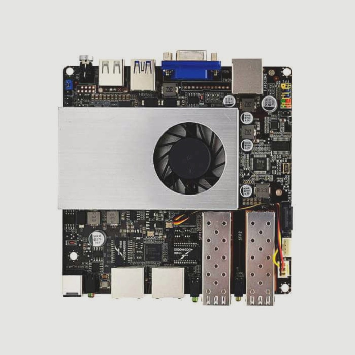
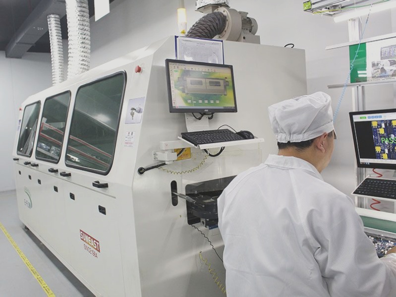
The PCB assembly technology consists of through-hole assembly (THT) and Surface-Mount Technology (SMT).
A printed circuit board (PCB) assembly refers to the process in which electronic components are securely mounted on a PCB. This process involves several steps, including surface-mount technology (SMT) or through-hole assembly (THT), depending on the components used.
Surface-Mount Technology (SMT)
SMT is the most common method used in PCB assembly. It involves placing components directly onto the PCB surface, eliminating the need for long leads or holes in the board. This assembly technique offers several advantages, such as higher component density, shorter assembly time, and improved reliability.
Through-Hole Technology (THT)
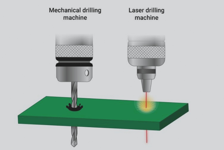
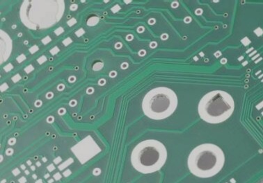
THT involves inserting components through holes in the PCB, which are then soldered to secure the components in place. This technique is often used for components with larger footprints or those without SMT alternatives. THT assembly requires careful alignment and manual soldering, which adds complexity to the assembly process.

1. Assembly Process
2. To assemble a PCB, the following steps are typically followed:

Quality Control
To ensure a high-quality PCB assembly, several key measures can be implemented:
1. Visual Inspection: The assembled PCB undergoes visual inspection to verify correct component placement and solder joints.
2. Electrical Testing: This phase evaluates the functionality and performance of the PCB assembly.
3. AOI (Automated Optical Inspection): Utilizing specialized machinery, AOI checks for defects like missing components or solder bridges.
4. X-RAY Inspection: An X-ray machine detects solder joint issues such as voids or splashes.
PCB assembly represents a pivotal stage in electronic manufacturing. Whether employing SMT or THT techniques, the process entails meticulous component selection, placement, soldering, and testing. Crucially, quality control practices—visual inspection, electrical testing, AOI, and X-ray inspection—are imperative to ensure a robust and reliable assembly.

What is a BOM list: A BOM list refers to the PCB materials necessary for the final specific printing of PCBA products. The circuit board company will procure these materials based on the BOM list provided by the customer. After passing the final soldering test, the product is then sent to the customer.
In China’s printed circuit board industry, the production of PCB bare boards and SMD assembly are typically handled separately. The PCB manufacturer produces the bare circuit boards and then transfers them to the SMT factory. Here, all the components specified in the BOM list are soldered onto the boards, transforming them into fully functional PCB products. Understanding the importance of the BOM list in this process is crucial for efficient PCB SMD assembly.
The BOM list plays a critical role in proper planning and ensuring smooth operations. It is essential for audits and facilitates tracking of purchased parts and inventory availability. It ensures that exact specifications or manufacturer preferences are met. In cases where this isn’t feasible, alternatives can be promptly discussed and proposed.
When creating a BOM list, several factors must be considered. It is advisable not to estimate the full quantity required upfront (e.g., 50 PCB components at a time). Instead, focus on the specific assembly requirements of the PCB, identifying the necessary components and their detailed specifications. This process is best handled by a team of experienced engineers who can accurately determine all required parts. The curated BOM list is then shared with the customer for verification.
A printed circuit board (PCB) assembly refers to the process in which electronic components are securely mounted on a PCB. This process involves several steps, including surface-mount technology (SMT) or through-hole assembly (THT), depending on the components used.
Surface-Mount Technology (SMT)
SMT is the most common method used in PCB assembly. It involves placing components directly onto the PCB surface, eliminating the need for long leads or holes in the board. This assembly technique offers several advantages, such as higher component density, shorter assembly time, and improved reliability.
Through-Hole Technology (THT)
THT involves inserting components through holes in the PCB, which are then soldered to secure the components in place. This technique is often used for components with larger footprints or those without SMT alternatives. THT assembly requires careful alignment and manual soldering, which adds complexity to the assembly process.
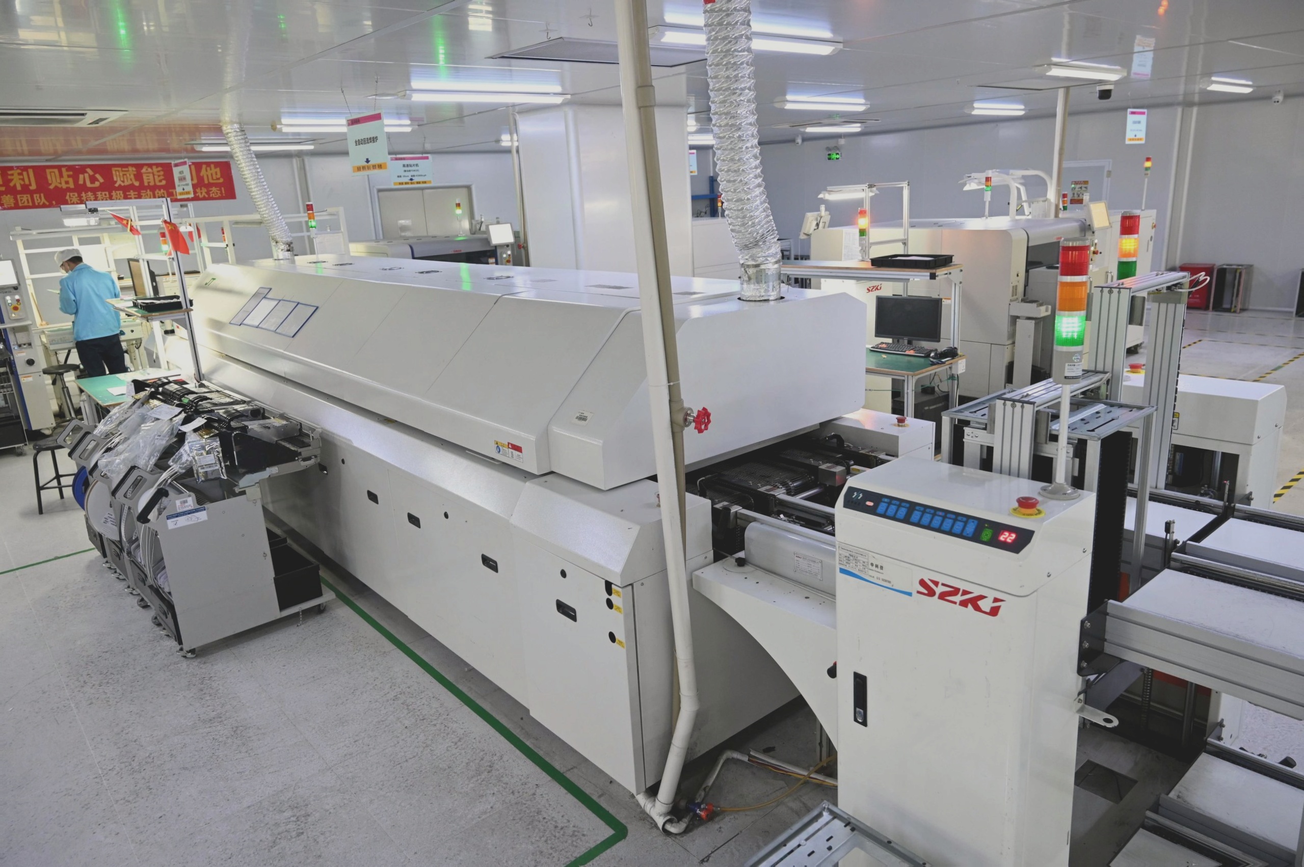
1. Assembly Process
2. To assemble a PCB, the following steps are typically followed:
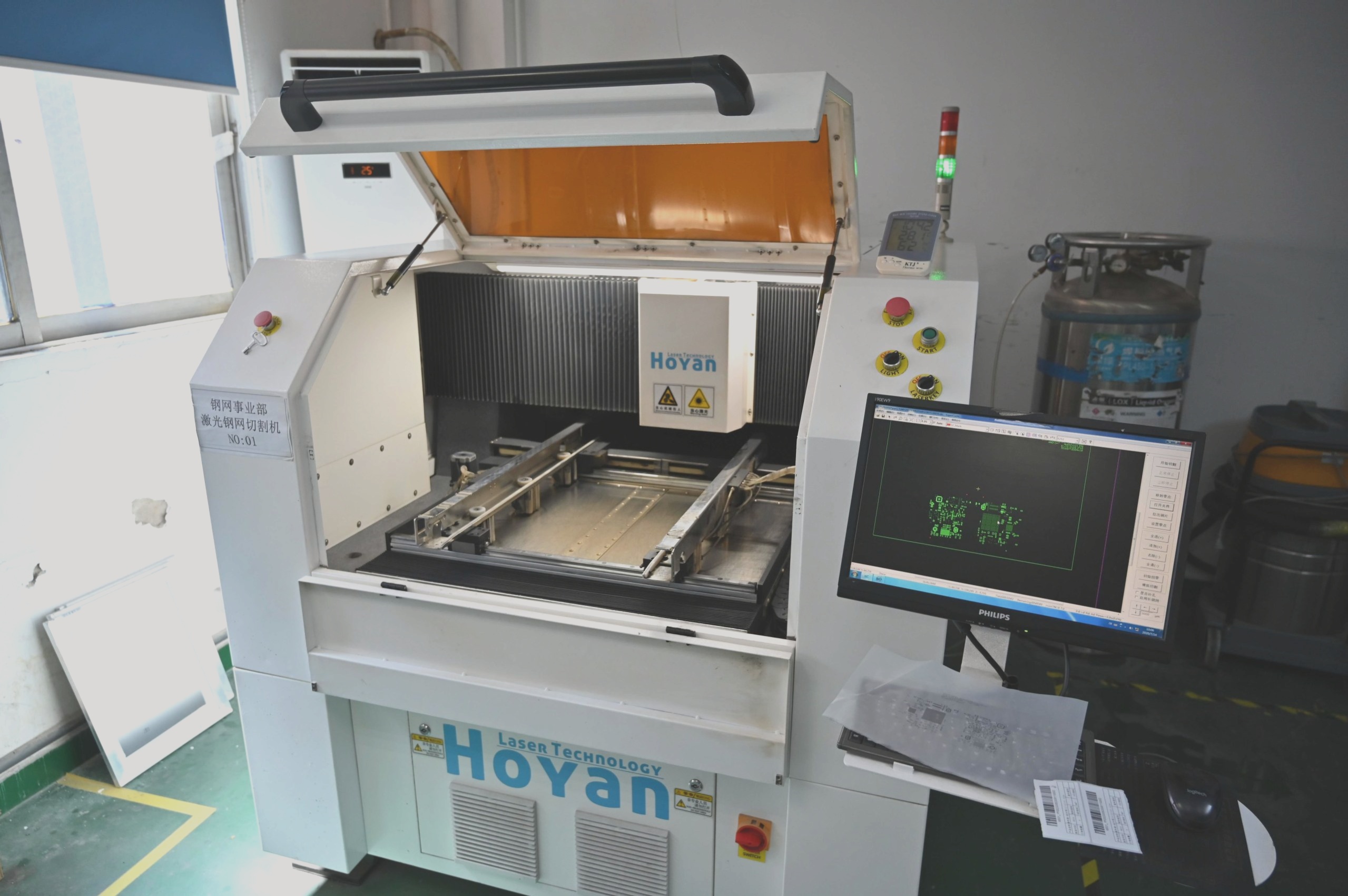
Quality Control
To ensure a high-quality PCB assembly, several key measures can be implemented:
1. Visual Inspection: The assembled PCB undergoes visual inspection to verify correct component placement and solder joints.
2. Electrical Testing: This phase evaluates the functionality and performance of the PCB assembly.
3. AOI (Automated Optical Inspection): Utilizing specialized machinery, AOI checks for defects like missing components or solder bridges.
4. X-RAY Inspection: An X-ray machine detects solder joint issues such as voids or splashes.
PCB assembly represents a pivotal stage in electronic manufacturing. Whether employing SMT or THT techniques, the process entails meticulous component selection, placement, soldering, and testing. Crucially, quality control practices—visual inspection, electrical testing, AOI, and X-ray inspection—are imperative to ensure a robust and reliable assembly.
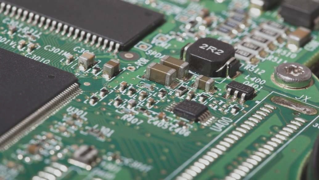
What is a BOM list: A BOM list refers to the PCB materials necessary for the final specific printing of PCBA products. The circuit board company will procure these materials based on the BOM list provided by the customer. After passing the final soldering test, the product is then sent to the customer.
In China’s printed circuit board industry, the production of PCB bare boards and SMD assembly are typically handled separately. The PCB manufacturer produces the bare circuit boards and then transfers them to the SMT factory. Here, all the components specified in the BOM list are soldered onto the boards, transforming them into fully functional PCB products. Understanding the importance of the BOM list in this process is crucial for efficient PCB SMD assembly.
The BOM list plays a critical role in proper planning and ensuring smooth operations. It is essential for audits and facilitates tracking of purchased parts and inventory availability. It ensures that exact specifications or manufacturer preferences are met. In cases where this isn’t feasible, alternatives can be promptly discussed and proposed.
When creating a BOM list, several factors must be considered. It is advisable not to estimate the full quantity required upfront (e.g., 50 PCB components at a time). Instead, focus on the specific assembly requirements of the PCB, identifying the necessary components and their detailed specifications. This process is best handled by a team of experienced engineers who can accurately determine all required parts. The curated BOM list is then shared with the customer for verification.
