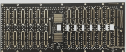
The backplane has long been a specialized product within the PCB manufacturing industry. Its design parameters differ significantly from those of most other circuit boards, and specific, often stringent, requirements must be met during production. Noise tolerance and signal integrity necessitate that backplane designs adhere to unique design rules. These characteristics result in substantial differences in equipment specifications, processing techniques, and other manufacturing requirements. As the demand for more advanced technology grows, future backplanes will become larger and more intricate, requiring unprecedented high clock frequencies and bandwidth capabilities. The number of signal lines (tracks) and nodes will continue to increase, and it will no longer be unusual for a backplane to include over 50,000 nodes.
1. User Requirements
The growing demand for increasingly complex, large-scale backplanes capable of operating at extremely high bandwidths has created a need for equipment processing capabilities that exceed those of conventional PCB manufacturing lines. Specifically, backplanes are becoming larger, heavier, and thicker, requiring more layers and perforations than standard PCBs. Additionally, the required line widths and tolerances are becoming more precise, and hybrid bus structures and assembly technologies are now essential.

**2. Requirements of the Size and Weight of the Backplane for the Conveying System**
The primary distinction between a conventional PCB and a backplane lies in the size and weight of the board, as well as the processing challenges associated with the large and heavy raw material substrate (panel). The standard size for PCB manufacturing equipment is typically 24×24 inches. However, users—particularly in the telecommunications sector—often require larger backplanes. This has driven the adoption of larger-sized board conveying systems. To address the routing challenges posed by large-pin-count connectors, designers must often add additional copper layers, which increases the number of backplane layers. Stringent EMC and impedance requirements further necessitate additional layers to ensure adequate shielding, reduce crosstalk, and improve signal integrity.
When high-power-consumption cards are inserted into the backplane, the copper layer thickness must be adjusted to provide sufficient current for proper card operation. These factors contribute to an increase in the average weight of the backplane, which in turn demands that conveyor belts and other handling systems not only be capable of safely transporting larger raw boards, but also account for the additional weight.
The need for thinner core layers and more layered backplanes creates two opposing requirements for the conveying system. On the one hand, conveyors must be capable of picking up and transporting large, thin boards with a thickness of less than 0.10 mm (0.004 inches) without causing damage. On the other hand, they must also support backplanes that are 10 mm (0.394 inches) thick and weigh 25 kg (56 pounds), ensuring that the board does not fall off during transport.
The difference in thickness between the inner layers (0.1 mm, or 0.004 inches) and the final backplane (up to 10 mm, or 0.39 inches) represents two orders of magnitude. This highlights the need for a conveying system robust enough to safely transport such boards through the manufacturing area. Since backplanes are thicker than conventional PCBs and feature a much larger number of holes, the process fluids can easily flow out. A 10 mm thick backplane with 30,000 holes, for example, can easily carry out a small amount of working fluid that is trapped in the guide holes by surface tension. To minimize fluid carry-out and eliminate any potential drying residues at the guide holes, it is crucial to clean the boreholes with high-pressure flushing and air blowers.
**3. Alignment of Layers**
As user applications demand more layers in the board design, the alignment between layers becomes critical. Interlayer alignment requires tight tolerance control, and the board size has placed even greater demands on this convergence. All layout processes are conducted in a temperature- and humidity-controlled environment, and exposure equipment operates in the same conditions. The alignment tolerance between the front and rear images across the entire area must be maintained at 0.0125 mm (0.0005 inches). To meet this precision requirement, a CCD camera is typically used to align the front and rear layers.
After etching, a four-drilling system is employed to perforate the inner plate. The perforation passes through the core plate with positional accuracy maintained at 0.025 mm (0.001 inch), and repeatability at 0.0125 mm (0.0005 inch). A pin is then inserted into the perforation to align the etched inner layers while bonding them together.
Originally, this post-etch perforation method ensured the alignment of the drilled holes and etched copper, forming a solid ring structure. However, as users demand more circuits in smaller areas for PCB routing, while keeping the fixed cost of the board unchanged, the etched copper plates must become smaller. This necessitates improved interlayer copper alignment. To achieve this, an X-ray drilling machine can be used. The machine can drill holes in boards up to 1092 x 813 mm (43 x 32 inches) with positional accuracy of 0.025 mm (0.001 inch). It has two primary uses:
1. To inspect the etched copper on each layer with an X-ray, determining the optimal drilling position.
2. To store statistical data on alignment deviations, feeding back this SPC (Statistical Process Control) data to earlier stages of production, such as material selection, processing parameters, and layout design, in order to minimize variation and continuously improve the process.
Though the electroplating process itself is similar to any standard plating procedure, two key differences must be considered due to the unique nature of large-format backplanes.
Fixtures and conveying systems must be capable of handling both large-sized and heavy boards. A raw material substrate of 1092 x 813 mm (43 x 32 inches) may weigh up to 25 kg (56 lbs). The board must be securely gripped during both transport and processing. The plating tank design must be deep enough to accommodate the board while ensuring uniform plating characteristics across the entire tank.
Since backplanes are thicker and heavier than conventional PCBs, they also have a larger heat capacity. Given the slow cooling rate of the backplane, the length of the reflow oven should be extended. Additionally, forced air cooling at the outlet is necessary to lower the temperature of the backplane to a safe operating level.
If your have any questions about PCB ,please contact me info@wellcircuits.com
1. User Requirements
The growing demand for increasingly complex, large-scale backplanes capable of operating at extremely high bandwidths has created a need for equipment processing capabilities that exceed those of conventional PCB manufacturing lines. Specifically, backplanes are becoming larger, heavier, and thicker, requiring more layers and perforations than standard PCBs. Additionally, the required line widths and tolerances are becoming more precise, and hybrid bus structures and assembly technologies are now essential.

**2. Requirements of the Size and Weight of the Backplane for the Conveying System**
The primary distinction between a conventional PCB and a backplane lies in the size and weight of the board, as well as the processing challenges associated with the large and heavy raw material substrate (panel). The standard size for PCB manufacturing equipment is typically 24×24 inches. However, users—particularly in the telecommunications sector—often require larger backplanes. This has driven the adoption of larger-sized board conveying systems. To address the routing challenges posed by large-pin-count connectors, designers must often add additional copper layers, which increases the number of backplane layers. Stringent EMC and impedance requirements further necessitate additional layers to ensure adequate shielding, reduce crosstalk, and improve signal integrity.
When high-power-consumption cards are inserted into the backplane, the copper layer thickness must be adjusted to provide sufficient current for proper card operation. These factors contribute to an increase in the average weight of the backplane, which in turn demands that conveyor belts and other handling systems not only be capable of safely transporting larger raw boards, but also account for the additional weight.
The need for thinner core layers and more layered backplanes creates two opposing requirements for the conveying system. On the one hand, conveyors must be capable of picking up and transporting large, thin boards with a thickness of less than 0.10 mm (0.004 inches) without causing damage. On the other hand, they must also support backplanes that are 10 mm (0.394 inches) thick and weigh 25 kg (56 pounds), ensuring that the board does not fall off during transport.
The difference in thickness between the inner layers (0.1 mm, or 0.004 inches) and the final backplane (up to 10 mm, or 0.39 inches) represents two orders of magnitude. This highlights the need for a conveying system robust enough to safely transport such boards through the manufacturing area. Since backplanes are thicker than conventional PCBs and feature a much larger number of holes, the process fluids can easily flow out. A 10 mm thick backplane with 30,000 holes, for example, can easily carry out a small amount of working fluid that is trapped in the guide holes by surface tension. To minimize fluid carry-out and eliminate any potential drying residues at the guide holes, it is crucial to clean the boreholes with high-pressure flushing and air blowers.
**3. Alignment of Layers**
As user applications demand more layers in the board design, the alignment between layers becomes critical. Interlayer alignment requires tight tolerance control, and the board size has placed even greater demands on this convergence. All layout processes are conducted in a temperature- and humidity-controlled environment, and exposure equipment operates in the same conditions. The alignment tolerance between the front and rear images across the entire area must be maintained at 0.0125 mm (0.0005 inches). To meet this precision requirement, a CCD camera is typically used to align the front and rear layers.
After etching, a four-drilling system is employed to perforate the inner plate. The perforation passes through the core plate with positional accuracy maintained at 0.025 mm (0.001 inch), and repeatability at 0.0125 mm (0.0005 inch). A pin is then inserted into the perforation to align the etched inner layers while bonding them together.
Originally, this post-etch perforation method ensured the alignment of the drilled holes and etched copper, forming a solid ring structure. However, as users demand more circuits in smaller areas for PCB routing, while keeping the fixed cost of the board unchanged, the etched copper plates must become smaller. This necessitates improved interlayer copper alignment. To achieve this, an X-ray drilling machine can be used. The machine can drill holes in boards up to 1092 x 813 mm (43 x 32 inches) with positional accuracy of 0.025 mm (0.001 inch). It has two primary uses:
1. To inspect the etched copper on each layer with an X-ray, determining the optimal drilling position.
2. To store statistical data on alignment deviations, feeding back this SPC (Statistical Process Control) data to earlier stages of production, such as material selection, processing parameters, and layout design, in order to minimize variation and continuously improve the process.
Though the electroplating process itself is similar to any standard plating procedure, two key differences must be considered due to the unique nature of large-format backplanes.
Fixtures and conveying systems must be capable of handling both large-sized and heavy boards. A raw material substrate of 1092 x 813 mm (43 x 32 inches) may weigh up to 25 kg (56 lbs). The board must be securely gripped during both transport and processing. The plating tank design must be deep enough to accommodate the board while ensuring uniform plating characteristics across the entire tank.
Since backplanes are thicker and heavier than conventional PCBs, they also have a larger heat capacity. Given the slow cooling rate of the backplane, the length of the reflow oven should be extended. Additionally, forced air cooling at the outlet is necessary to lower the temperature of the backplane to a safe operating level.
If your have any questions about PCB ,please contact me info@wellcircuits.com


