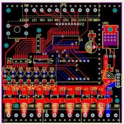
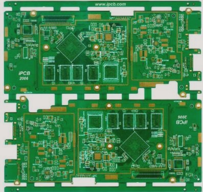
Effectively control the entire hardware development process for PCB board design and development to ensure that the resultant PCB controller hardware meets customer requirements and relevant national standards.
Scope
This role encompasses the development of new controller products and the enhancement of finalized products.
Duties
When there is a need for control board design and development, a dedicated development team is formed. This team comprises product development supervisors, hardware engineers, test engineers, and reliability engineers.
The product development supervisor oversees the preparation and execution of the project development plan. They also organize, coordinate, and manage the design and development processes, including arranging design reviews, conducting design verification, and finalizing the design.
The hardware engineer handles the selection, design, PCB board layout, and hardware circuit debugging. The test engineer is responsible for testing hardware circuit prototypes and finished products.

The reliability engineer is tasked with designing and verifying the hardware circuit for reliability.
Establishment of the Development Team:
The PCB product development supervisor forms a hardware development team based on project requirements and drafts the “Hardware Product Development Plan”. This plan is executed post-approval from higher authorities and covers:
– Phases of design and development.
– Comprehensive activities for PCB design review, verification, confirmation, and necessary materials.
– Tasks, responsible parties, and schedule for each phase.
The “Development Plan” must be regularly updated to reflect design progress adjustments, approved by the project team, and reported to superiors.
There are five methods for PCB soldering, each with unique advantages:
Solution 1: Manual Soldering
Manual soldering suits product trials, small batch electronic production, debugging, maintenance, and scenarios unsuitable for automated soldering. It demands basic tools, simple steps, and easy mastery, ideal when dealing with few electronic component pins.
Solution 2: Dip Soldering
Dip soldering offers straightforward operation and high efficiency but risks defects like false soldering. Correcting solder joints demands precision in solder bath temperature control to prevent board warping or component damage. It necessitates advanced soldering tools, making it less cost-effective for students.
Solution 3: Wave Soldering
Wave soldering provides high efficiency, best suited for large-scale single-sided PCB soldering. Although controllable in terms of solder temperature, duration, type, and flux, it can lead to solder bridge formation, requiring rework. This method demands sophisticated tools, making it less suitable for student learning.
Solution 4: Reflow Soldering
Reflow soldering is chiefly for SMD components, minimizing thermal stress and ensuring high-quality solder joints without bridging issues. It requires advanced soldering tools, posing challenges for quick mastery and affordability among students.
Solution 5: PCB Contact Welding (Wuxi Welding)
This method is practical for connecting cables to PCB terminals but holds no value for radio PCB welding and is not cost-effective for students.
Scope
This role encompasses the development of new controller products and the enhancement of finalized products.
Duties
When there is a need for control board design and development, a dedicated development team is formed. This team comprises product development supervisors, hardware engineers, test engineers, and reliability engineers.
The product development supervisor oversees the preparation and execution of the project development plan. They also organize, coordinate, and manage the design and development processes, including arranging design reviews, conducting design verification, and finalizing the design.
The hardware engineer handles the selection, design, PCB board layout, and hardware circuit debugging. The test engineer is responsible for testing hardware circuit prototypes and finished products.

The reliability engineer is tasked with designing and verifying the hardware circuit for reliability.
Establishment of the Development Team:
The PCB product development supervisor forms a hardware development team based on project requirements and drafts the “Hardware Product Development Plan”. This plan is executed post-approval from higher authorities and covers:
– Phases of design and development.
– Comprehensive activities for PCB design review, verification, confirmation, and necessary materials.
– Tasks, responsible parties, and schedule for each phase.
The “Development Plan” must be regularly updated to reflect design progress adjustments, approved by the project team, and reported to superiors.
There are five methods for PCB soldering, each with unique advantages:
Solution 1: Manual Soldering
Manual soldering suits product trials, small batch electronic production, debugging, maintenance, and scenarios unsuitable for automated soldering. It demands basic tools, simple steps, and easy mastery, ideal when dealing with few electronic component pins.
Solution 2: Dip Soldering
Dip soldering offers straightforward operation and high efficiency but risks defects like false soldering. Correcting solder joints demands precision in solder bath temperature control to prevent board warping or component damage. It necessitates advanced soldering tools, making it less cost-effective for students.
Solution 3: Wave Soldering
Wave soldering provides high efficiency, best suited for large-scale single-sided PCB soldering. Although controllable in terms of solder temperature, duration, type, and flux, it can lead to solder bridge formation, requiring rework. This method demands sophisticated tools, making it less suitable for student learning.
Solution 4: Reflow Soldering
Reflow soldering is chiefly for SMD components, minimizing thermal stress and ensuring high-quality solder joints without bridging issues. It requires advanced soldering tools, posing challenges for quick mastery and affordability among students.
Solution 5: PCB Contact Welding (Wuxi Welding)
This method is practical for connecting cables to PCB terminals but holds no value for radio PCB welding and is not cost-effective for students.

