1. Introduction to PCB
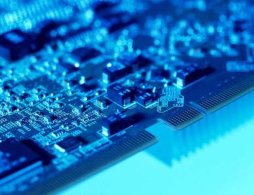
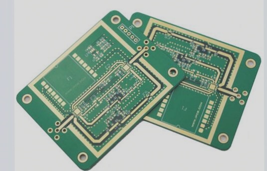
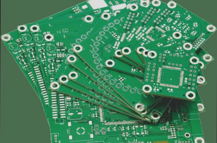
PCB, or printed circuit board, is an essential electronic component that serves as a support structure and provides electrical connections for electronic components. The term “printed” originates from its manufacturing process involving electronic printing. The inventor of the PCB was Austrian Paul Eisler, who first utilized it in a radio unit in 1936. Subsequently, the technology gained significant use in American military radios by 1943. In 1948, the United States formally recognized its commercial potential. PCB technology began to be widely adopted from the mid-1950s onwards. Prior to PCBs, electronic components were interconnected through direct wire connections. Today, PCBs have become indispensable in the electronics industry, replacing circuit panels as effective experimental tools. PCBs are classified based on the number of circuit layers: single-sided, double-sided, and multi-layer boards. Common multi-layer boards typically range from 4 to 6 layers, while complex multi-layer boards can exceed ten layers.

1. There are three main types of PCB boards:
1) Single panel
A single-sided board has components concentrated on one side and wiring on the other. Because it has wiring on only one side, it is called single-sided. Due to strict circuit design constraints, this type was primarily used in early circuits.
2) Double panel
A double-sided board has wiring on both sides, connected through vias. Vias are small holes filled or coated with metal that allow connections between the two sides. This design, with its increased area and interleaved wiring, suits more complex circuits than single-sided boards.
3) Multilayer board
Multilayer boards enhance wiring area by stacking multiple single or double-sided boards. These boards consist of inner layers (double-sided or single-sided), outer layers, and insulating materials, interconnected through a positioning system and conductive patterns. Boards with four to six layers, known as multi-layer PCBs, are common, although technically, PCBs with nearly 100 layers exist. While layer count isn’t readily visible, it can be discerned on close inspection.
PCBs are categorized as ordinary or flexible based on softness and rigidity. PCBs serve as the foundation for circuit components in electronic devices, providing electrical connections crucial to device performance. As microelectronics advance, component density on PCBs increases, demanding more stringent electromagnetic compatibility (EMC) designs to ensure system stability.
2. Common EMI in PCB
To address electromagnetic compatibility in PCB design, two methods are used: active reduction and passive compensation. This involves analyzing sources and paths of electromagnetic interference (EMI). Typical EMI in PCBs includes conducted interference, crosstalk interference, and radiated interference.
2.1 Conducted interference
Conducted interference affects circuits through wire coupling and common mode impedance. For instance, noise entering via a power supply circuit can affect all connected circuits, as shown in Figure 1.
2.2 Crosstalk interference
Crosstalk occurs when one signal line interferes with adjacent paths due to mutual capacitance and inductance. Proper management is essential to prevent signal degradation.
2.3 Radiated interference
Radiated interference results from electromagnetic wave radiation, affecting nearby traces and cables. Field-to-line coupling can induce unwanted currents, complicating PCB design.
3. PCB Electromagnetic Compatibility Design
As electronic component and circuit densities increase, ensuring PCB designs meet EMC standards is critical for system reliability.
3.1 Selection of PCB board
Design considerations include PCB size, layer count, signal density, and frequency. Balancing these factors optimizes EMC while managing production costs.
3.2 PCB layout design
Layout principles aim to minimize interference between components, optimize signal paths, and ensure thermal management. Careful arrangement and isolation of components mitigate interference risks.
3.3 Component layout design
Integrated circuits are preferred for reliability and reduced interference. Grouping and spacing components based on function enhances layout efficiency.
3.4 PCB wiring design
Wiring strategies prioritize signal integrity and impedance control, minimizing noise and ensuring reliable data transmission.
3.5 Power line design of PCB board
Power lines are designed to minimize resistance and noise, enhancing system stability and performance.
3.6 Ground wire design of PCB board
Effective grounding strategies mitigate ground loop interference and ensure signal integrity across digital and analog circuits.
3.7 Layout of crystal oscillator circuit on PCB board
Optimal placement and layout of high-frequency components like crystal oscillators reduce noise and interference.
3.8 Electrostatic protection design of PCB board
Measures include component selection, signal path design, and use of protective devices to safeguard against electrostatic discharge (ESD).
4. Conclusion
Effective PCB electromagnetic compatibility design reduces external radiation and improves resistance to interference, crucial for high-speed PCB applications. These strategies, while comprehensive, must adapt to specific design goals and conditions for optimal EMC performance.
PCB, or printed circuit board, is an essential electronic component that serves as a support structure and provides electrical connections for electronic components. The term “printed” originates from its manufacturing process involving electronic printing. The inventor of the PCB was Austrian Paul Eisler, who first utilized it in a radio unit in 1936. Subsequently, the technology gained significant use in American military radios by 1943. In 1948, the United States formally recognized its commercial potential. PCB technology began to be widely adopted from the mid-1950s onwards. Prior to PCBs, electronic components were interconnected through direct wire connections. Today, PCBs have become indispensable in the electronics industry, replacing circuit panels as effective experimental tools. PCBs are classified based on the number of circuit layers: single-sided, double-sided, and multi-layer boards. Common multi-layer boards typically range from 4 to 6 layers, while complex multi-layer boards can exceed ten layers.

1. There are three main types of PCB boards:
1) Single panel
A single-sided board has components concentrated on one side and wiring on the other. Because it has wiring on only one side, it is called single-sided. Due to strict circuit design constraints, this type was primarily used in early circuits.
2) Double panel
A double-sided board has wiring on both sides, connected through vias. Vias are small holes filled or coated with metal that allow connections between the two sides. This design, with its increased area and interleaved wiring, suits more complex circuits than single-sided boards.
3) Multilayer board
Multilayer boards enhance wiring area by stacking multiple single or double-sided boards. These boards consist of inner layers (double-sided or single-sided), outer layers, and insulating materials, interconnected through a positioning system and conductive patterns. Boards with four to six layers, known as multi-layer PCBs, are common, although technically, PCBs with nearly 100 layers exist. While layer count isn’t readily visible, it can be discerned on close inspection.
PCBs are categorized as ordinary or flexible based on softness and rigidity. PCBs serve as the foundation for circuit components in electronic devices, providing electrical connections crucial to device performance. As microelectronics advance, component density on PCBs increases, demanding more stringent electromagnetic compatibility (EMC) designs to ensure system stability.
2. Common EMI in PCB
To address electromagnetic compatibility in PCB design, two methods are used: active reduction and passive compensation. This involves analyzing sources and paths of electromagnetic interference (EMI). Typical EMI in PCBs includes conducted interference, crosstalk interference, and radiated interference.
2.1 Conducted interference
Conducted interference affects circuits through wire coupling and common mode impedance. For instance, noise entering via a power supply circuit can affect all connected circuits, as shown in Figure 1.
2.2 Crosstalk interference
Crosstalk occurs when one signal line interferes with adjacent paths due to mutual capacitance and inductance. Proper management is essential to prevent signal degradation.
2.3 Radiated interference
Radiated interference results from electromagnetic wave radiation, affecting nearby traces and cables. Field-to-line coupling can induce unwanted currents, complicating PCB design.
3. PCB Electromagnetic Compatibility Design
As electronic component and circuit densities increase, ensuring PCB designs meet EMC standards is critical for system reliability.
3.1 Selection of PCB board
Design considerations include PCB size, layer count, signal density, and frequency. Balancing these factors optimizes EMC while managing production costs.
3.2 PCB layout design
Layout principles aim to minimize interference between components, optimize signal paths, and ensure thermal management. Careful arrangement and isolation of components mitigate interference risks.
3.3 Component layout design
Integrated circuits are preferred for reliability and reduced interference. Grouping and spacing components based on function enhances layout efficiency.
3.4 PCB wiring design
Wiring strategies prioritize signal integrity and impedance control, minimizing noise and ensuring reliable data transmission.
3.5 Power line design of PCB board
Power lines are designed to minimize resistance and noise, enhancing system stability and performance.
3.6 Ground wire design of PCB board
Effective grounding strategies mitigate ground loop interference and ensure signal integrity across digital and analog circuits.
3.7 Layout of crystal oscillator circuit on PCB board
Optimal placement and layout of high-frequency components like crystal oscillators reduce noise and interference.
3.8 Electrostatic protection design of PCB board
Measures include component selection, signal path design, and use of protective devices to safeguard against electrostatic discharge (ESD).
4. Conclusion
Effective PCB electromagnetic compatibility design reduces external radiation and improves resistance to interference, crucial for high-speed PCB applications. These strategies, while comprehensive, must adapt to specific design goals and conditions for optimal EMC performance.


