Common Mistakes in PCB Board Schematic Diagrams:
-
The ERC pin has no access signal:
- Ensure I/O attributes are defined for the pins when creating the package.
- Modify inconsistent grid properties when creating or placing components and connect the pins and lines accordingly.
- Ensure the pin direction is correct when creating a component and connect it to the non-pin name end.
-
The component exceeds the drawing bounds:
Ensure the component is created in the center of the drawing paper in the component library.
-
The project file netlist can only be partially transferred to the PCB board:
Select global when generating the netlist.
-
Avoid using annotate with self-created multi-part components.
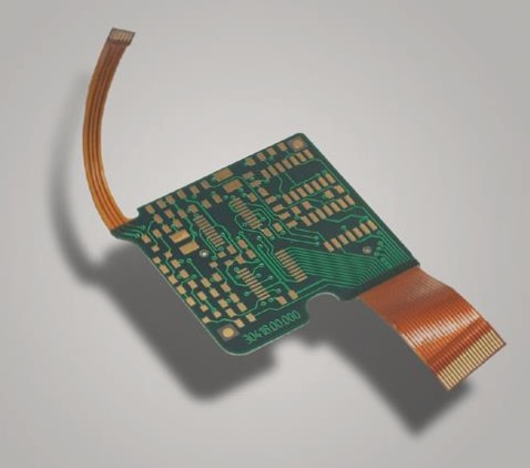
Common Mistakes in PCB Board:

-
NODE is not found when the network is loaded:
- The components in the schematic diagram use packages that are not in the PCB library.
- The components in the schematic diagram use packages with inconsistent names in the PCB library.
- The components in the schematic diagram use packages with inconsistent pin numbers in the PCB library. For example, a triode may have pin numbers labeled as e, b, c in the schematic but 1, 2, 3 in the PCB board.
-
When printing, it cannot always be printed on one page:
- It is not at the origin when creating the PCB library.
- The component has been moved and rotated many times, resulting in hidden characters outside the PCB board boundary. To resolve this, select to show all hidden characters, shrink the PCB board, and move the characters within the boundaries.
-
The DRC network is divided into several parts:
This indicates that the network is not connected. To resolve this issue, examine the file and use CONNECTED COPPER to locate the disconnected part.
PCB Board Wiring Design:
In PCB board design, wiring is a crucial step in completing product design. The process includes single-sided, double-sided, and multi-layer wiring, as well as automatic and interactive routing. Ground wire isolation should be added if necessary, and wiring on two adjacent layers should be perpendicular to prevent parasitic coupling.
Handling of Power and Ground Wires:
Proper wiring of power and ground wires is essential to minimize noise interference and ensure product quality.
Common Ground Processing of Digital Circuits and Analog Circuits:
Separate digital and analog grounds within the board but connect at the interface with the outside world. Different grounds on the PCB board should be established based on system design.
Routing on the Electrical (Ground) Layer:
In multi-layer printed board wiring, routing on the electrical (ground) layer can optimize board space and reduce production costs.
Handling of Connecting Legs in Large Area Conductors:
Using thermal pads when connecting components in large grounding areas can help reduce the risk of virtual solder joints caused by excessive heat dissipation during welding.