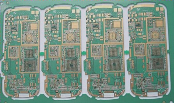
The Challenges and Considerations of Spliced PCB Boards
Splicing boards in PCB fabrication is often done to cut down on production costs. However, there are several key factors to keep in mind to ensure optimal results:
- Production Line Variation: The choice of production line can impact costs, especially for PCB panels within a certain width range. Different lines may require specific materials, affecting processing speed.
- Outer Frame Design: Careful attention should be paid to the outer frame of the PCB panel to avoid deformation. Avoiding V grooves on this side and maintaining consistent orientation is crucial.
- Connector Extension: Adequate extension between boards and frames is essential to facilitate tool separation post-welding.
- Positioning Accuracy: Having at least three positioning points on the board’s edge helps determine reference coordinates accurately for processing and board level.
- Reference Positioning Points: Maintain a 5mm distance from the edge, with a 1.5mm non-resistance area around each point to prevent interference with other components.
- Positioning Holes: Each small board should have at least three positioning holes without any wiring or components within 1mm to avoid errors.
- Design Considerations: While spliced PCB boards can cut costs and improve processing speed, meticulous design scrutiny is crucial to avoid potential issues in later stages.
By addressing these challenges and considerations effectively, manufacturers can harness the benefits of spliced PCB boards while ensuring quality and efficiency in production processes.