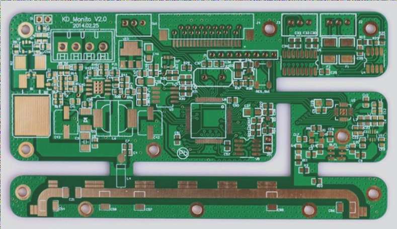
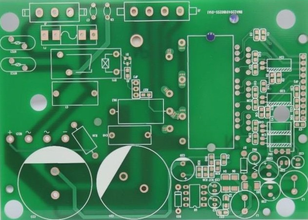
1. PCB circuit board connection is a wire bonding method in the chip production process. It is generally used to connect the internal circuits of a chip with gold or aluminum wires to the packaging pins or before bonding the gold-plated copper foil of the circuit board. Ultrasonic generators (usually 40-140KHz) generate high-frequency vibrations through transducers and transmit them to wedges through horns. When the wedge body comes into contact with the lead and welding parts, it is subjected to pressure and vibration, causing the metal surfaces to be welded to rub against each other, damaging the oxide film, and undergoing plastic deformation, resulting in close contact between the two pure metal surfaces, achieving atomic distance bonding, and ultimately forming a solid mechanical connection. Usually, after soldering (i.e. circuit and pin connections), the chip is packaged with black glue.

2 Welding process requirements:

1) Clean PCB circuit board: Wipe off oil, dust, and oxide layer on the board, then use a brush to clean the wiped surface or blow it away with an air gun.

2) Glue dripping: Apply an appropriate amount of glue to the four corners of the board, with four glue points. Glue can only be applied to the four corners of the board, and excessive glue or glue on other parts of the board can affect its normal operation.

3) Chip mounting (solid crystal): When using a vacuum suction pen, the suction nozzle must be flat to avoid scratching the surface of the chip. Check the orientation of the chip and ensure that it is “flat, stable, and straight” when attached to the PCB circuit board: flat refers to the chip being parallel to the PCB, and there is no gap between the chips and the board; The stable chip and PCB circuit board will not fall off throughout the entire process; Stick the chip vertically to the reserved position on the PCB without deviation. The chip cannot be upside down or upside down.

4) Bonding: Through tensile testing, the qualified PCB bonding strength is: 1.0 wire ≥ 3.5G, 1.25 wire ≥ 4.5G. Standard aluminum wire solder joint requirements: wire tail ≥ 0.3 times wire diameter, ≤ 1.5 times wire diameter. The shape of the solder joint is elliptical. Solder joint length ≥ 1.5 times wire diameter, ≤ 5.0 times wire diameter. Solder joint width ≥ 1.2 times wire diameter, ≤ 3.0 times wire diameter. The bonding process requires careful operation, and the solder joints must be accurate. The operator should observe the welding process under a microscope to check for defects such as broken keys, entanglement, deviation, cold welding and hot welding, and aluminum sheet lifting. Once any problems are found, the responsible technician should be notified immediately for resolution.

5) Sealing: Before installing the chip plastic ring, check the regularity of the plastic ring to ensure that there is no obvious deformation in the center. Ensure that the bottom of the plastic ring is tightly attached to the surface of the chip during installation, and that the photosensitive area at the center of the chip is not obstructed. When dripping, ensure that the black glue completely covers the aluminum wires of the PCB sun ring and bonding chip, and the wires should not be visible. Black glue should not overflow the PCB sun ring, and any overflow should be wiped off in a timely manner. Black glue cannot penetrate the wafer through the plastic ring. During the dispensing process, the needle or cotton swab should not touch the surface of the chip or solder wire inside the plastic ring. Strictly control the drying temperature: preheat at 120 ± 5 ℃ for 1.5-3.0 minutes; Dry at 140 ± 5 ℃ for 40-60 minutes. After drying, there should be no pores or uncured phenomenon on the surface of ethylene, and the height of ethylene should not be higher than the plastic ring.

6) Testing: Using a combination of multiple testing methods: A. Visual and manual inspection; B. Quality inspection of automatic welding line for bonding machine; C. Automatic Optical Image Analysis (AOI) and X-ray analysis are used to check the quality of internal solder joints]>
PCB circuit board connection via ultrasonic bonding is a chip manufacturing process, involving high-frequency vibration to create a robust mechanical bond between internal circuitry and external leads or bonding pads, followed by encapsulation with black adhesive, while soldering process requires meticulous cleanliness, accurate chip placement, careful bonding, thorough sealing, and comprehensive testing.
PCB circuit board, wire bonding, ultrasonic generator, soldering process, sealing process


PCBA Processing: Common Issues Solutions
SMT patch processing stands as the linchpin of SMT procedures, where the pace of patch processing frequently imposes constraints on production line capacity. To furnish an SMT chip processing assembly line, one must equip it with at least one high-speed chip placement machine for mounting conventional size components alongside a multi-functional chip placement machine tailored for special size components. Throughout the course of SMT patch processing, an array of challenges invariably emerges. Herein, the editor of Zhongke Circuit Board Factory delineates the genesis and remedies for these ubiquitous quandaries.
1. Poor Wetting in PCBA Processing
Phenomenon: Lack of reaction between the substrate solder area and the metal ensues during soldering, leading to deficient or absent soldering.
Cause Analysis:
(1) Gas presence on the substrate surface during wave soldering undermines wetting.
(2) Flux activity dwindles and wetting suffers when solder contains over 0.005% residual metal.
(3) Contamination on the welding area surface, flux residue, or formation of metal compounds on chip component surfaces precipitates poor wetting. Instances include sulfide and oxide formation on silver and tin surfaces, respectively.
Solutions:
(1) Adhere rigorously to welding protocols and guidelines.
(2) Ensure cleanliness of PCB circuit boards and components.
(3) Opt for appropriate solder, and configure soldering temperature and duration judiciously.
2. Tombstoning
Phenomenon: One end of the component fails to contact the pad, either standing upright or barely touching it.
Cause Analysis:
(1) Solder paste’s wettability influences tombstoning.
(2) Certain electronic component shapes are predisposed to tombstoning.
(3) Uneven heating and rapid temperature escalation during reflow soldering contribute to tombstoning.
(4) Incorrect solder paste selection, absence of preheating prior to soldering, and erroneous sizing of soldering areas exacerbate tombstoning.
PCBA Processing Solutions:
1. Adjust solder printing thickness prudently.
2. Calibrate reflow soldering zone temperature ramp-up appropriately.
3. Handle electronic components in accordance with storage and retrieval guidelines.
4. Mitigate component end surface tension upon solder melting.
5. Preheat PCB circuit boards to ensure uniform heating during soldering.

Leave a Comment

Contact

WellCircuits
More than PCB

Upload your GerberFile(7z,rar,zip)