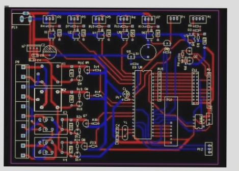
PCB Anti-Interference Design Methods
-
Power Trace Design
Increasing the width of power traces on a printed circuit board can help reduce loop resistance and improve noise immunity. Aligning power and ground traces with the direction of data transmission is also beneficial.
-
Ground Wire Design Principles
-
Separation of Digital and Analog Grounds
Separating the grounds of logic circuits and analog circuits on the same PCB is recommended. Ground traces should be short and direct, with a large-area ground plane around high-frequency components to minimize noise.
-
Thickness of Ground Trace
Ground traces should be wide enough to handle expected currents to avoid voltage fluctuations. Ideally, the trace width should be at least 2–3 mm.
-
Closed Loop Grounding
For PCBs with digital circuits, arranging the grounding circuit in a loop can enhance noise resistance and anti-interference performance.
-
-
Decoupling Capacitor Placement
Decoupling capacitors play a crucial role in PCB design. Key principles for their placement include connecting appropriate capacitors across power inputs, using ceramic capacitors for integrated circuit chips, and employing decoupling capacitors for components like RAM and ROM storage devices.
Short leads for high-frequency bypass capacitors and the use of RC circuits for components generating spark discharges are also recommended.
-
PCB Routing Guidelines
Routing is a critical step in PCB design, requiring skill and effort. Avoid placing input and output terminals adjacent or parallel to each other to prevent reflection interference. Ground traces can be used for isolation, and traces on adjacent layers should cross at right angles to minimize parasitic coupling.
Predefined routing rules and optimization of global routing are essential for successful automatic routing.
Modern PCB Design Strategies
In today’s high-density PCB designs, traditional through-hole vias are being phased out in favor of blind and buried vias. These advanced via technologies offer the same functionality as traditional vias but save valuable routing space, leading to improved routing efficiency and a smoother design process.
1. Importance of Power and Ground Plane Management
Effective routing is crucial in PCB design, but proper handling of power and ground planes is equally important. Failure to manage these planes correctly can introduce noise, impacting product performance and yield. Engineers must pay close attention to power and ground trace routing to minimize noise interference and ensure high-quality products.
2. Grounding Strategies for Digital and Analog Circuits
Modern PCBs often combine digital and analog circuits, requiring careful consideration of potential interference between the two. Digital circuits operating at high frequencies can generate noise, while analog circuits are sensitive to interference. To minimize interference, separate the digital and analog grounds within the board, connecting them only at a single point. This isolation helps reduce noise and ensures optimal circuit performance.
3. Efficient Signal Routing on Power and Ground Layers
In multi-layer PCB designs, signal layers can become congested, making additional signal routing challenging. To address this issue, consider routing signals on power and ground layers. Prioritize power layers followed by ground layers to maintain circuit integrity and reduce interference.
4. Best Practices for Connecting Component Leads to Ground Planes
Connecting component leads to large ground planes requires a comprehensive approach for optimal electrical performance. Directly connecting component pads to the copper plane is ideal but can pose challenges during soldering. To enhance soldering reliability, use crosshatched pads, also known as thermal pads, to distribute heat effectively and reduce the risk of cold solder joints. This approach ensures reliable connections in multi-layer PCBs and streamlines the assembly process.