The Evolution of PCBs in the 5G Era
With the global shift to 5G technology, mini 5G base stations are now ubiquitous, installed every 100 meters in urban areas on various structures. Unlike the distant placement of 4G LTE towers, these base stations are crucial for the high-speed, low-latency 5G network.
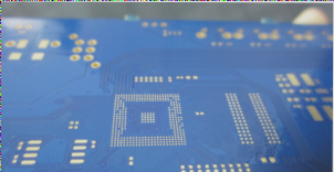
Advanced Materials for 5G PCBs
- New materials like fast laminates with low dielectric constants (Dk) are essential for 5G base stations operating at 28 GHz, reducing transmission loss by up to 30%.
- High-precision impedance control with tight tolerance levels of ±5% demands accurate PCB circuit dimensions and consistent internal measurements.
- Advanced production techniques such as Direct Imaging (DI) and Automated Optical Inspection (AOI) are crucial for meeting stringent quality standards.
Server Design for 5G Communication
Both local and central servers collaborate to support the 5G network, with edge computing enhancing efficiency by processing real-time data at the network edge.
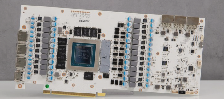
High-Performance PCB Designs
- PCBs for 5G servers range from 12 to 30 layers, requiring careful engineering for strict impedance control to handle high frequencies.
- Proper impedance management is vital for signal integrity and reliable communication as 5G frequencies increase.
5G Smartphone Manufacturing
Next-gen 5G smartphones utilize mSAP and SLP technologies for efficient signal transmission and power reduction, incorporating flexible and rigid-flex combined PCBs and MIMO antenna systems with AiP technology for enhanced performance.
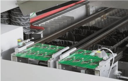
Advanced Technologies in PCB Manufacturing for 5G Components
Modern PCB manufacturing processes for 5G components require advanced AOI systems with laser hole detection for precise positioning and high-quality connections. In particular, mSAP/SLP and flexible PCBs demand sophisticated DI systems for accurate line patterning and high DoF capabilities for production quality maintenance.
These cutting-edge technologies not only ensure fine line patterning but also boost productivity, crucial for meeting the increasing demand for 5G smartphone components. Automated optical shaping and repair systems further enhance production efficiency by addressing defects identified during inspections.
Enhancing 5G Infrastructure with Innovative PCB Design
By embracing state-of-the-art manufacturing technologies like direct laser imaging (DLI), automated optical inspection (AOI), and automated optical shaping and repair, PCB designers can effectively address the challenges posed by 5G infrastructure requirements.
These key processes play a vital role in overcoming obstacles such as low latency, high-frequency needs, and the utilization of intricate and delicate materials. Moreover, they not only facilitate the design and production of 5G components but also improve yields in mass production settings, essential for the successful deployment and operation of 5G networks.