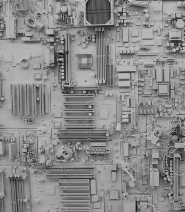
The so-called “Copper Coating” refers to using the unused space on a circuit board as a base surface, and then filling it with solid copper, creating areas known as copper fills. The significance of copper coating is to reduce ground impedance, improve anti-interference ability, reduce voltage drop and improve power efficiency, as well as reduce loop area when connected with the ground wire. Additionally, copper coating is important for maintaining PCB welding without deformation. Most PCB manufacturers require PCB designers to fill open areas of the PCB with copper or grid-like ground wire. Improper handling of copper coating can lead to negative effects, particularly in high frequency circuits where distributed capacitance of wiring can cause antenna effects and emit noise outward. Therefore, it is crucial to ensure proper treatment of copper coating to increase current and shield interference.
There are two basic forms of copper coating – large area copper coating and grid copper coating. It is not possible to generalize which form is better as each has its own advantages and disadvantages. Large area copper coating has the dual role of increasing current and shielding, but over wave soldering, it may cause the board to tilt up or even foam. Therefore, several slots are generally opened in a large area copper coating to alleviate foaming of copper foil. On the other hand, grid copper coating primarily provides a shielding effect, but reduces the role of increasing current. From a heat dissipation perspective, the grid has advantages and also plays a role in electromagnetic shielding. The grid is composed of staggered directions, and the width of the lines has corresponding “electrical lengths” for the working frequency of the circuit board. For high frequency circuits, the grid is recommended for interference requirements, while low frequency and high current circuits commonly use complete copper paving. It is important to choose the appropriate form of copper coating based on the design of the circuit board and not hold onto one form over the other.


