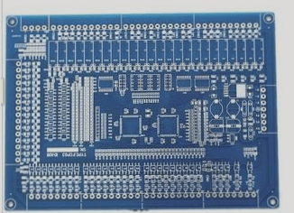
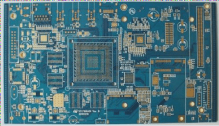
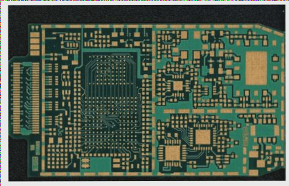
In the circuit board layout process, once the system layout is completed, it is essential to review the PCB diagram to assess the reasonableness of the layout and whether optimal performance can be achieved. This can typically be evaluated from the following aspects:
1. Whether the system layout ensures reasonable or optimal routing, whether the connections can be made reliably, and whether the circuit’s operational reliability can be assured. During the layout process, it is crucial to maintain an overall perspective on the direction of signals, as well as the power supply and ground network.
2. Whether the dimensions of the printed board align with those of the processing drawing, whether they meet the requirements of the PCB manufacturing process, and whether there are proper reference marks. This aspect requires particular attention. Many PCB designs may appear aesthetically pleasing and logically structured, but if the positioning of the connectors is not accurately defined, it can lead to issues in integrating the circuit with other systems.

3. Assess whether the components conflict in both two-dimensional and three-dimensional spaces. It’s crucial to pay attention to the actual dimensions of the devices, particularly their height. When soldering components without a designated layout, the height should typically not exceed 3mm.
4. Evaluate whether the layout of the components is dense yet orderly, with a neat arrangement and all components properly positioned. In component layout, considerations should include not only the signal direction and type but also any areas requiring special attention or protection. Additionally, the overall density of the device layout must be balanced to ensure uniformity.
5. Determine if components that require frequent replacement can be easily accessed, and whether the plug-in board can be effortlessly inserted into the equipment. It’s essential to ensure the convenience and reliability of replacing and connecting frequently swapped components.
6. Check the ease of adjusting adjustable components.
7. Ensure there is an appropriate distance between thermal elements and heating components.
8. Verify that a heatsink or fan is installed where heat dissipation is necessary, and ensure that airflow is unobstructed. Attention should be given to the heat management of components and circuit boards.
9. Confirm that the signal paths are smooth and that interconnections are as short as possible.
10. Assess whether plugs, sockets, and other connectors align with the mechanical design.
11. Consider if there is potential for line interference.
12. Ensure that the mechanical strength and performance of the circuit board have been taken into account.
13. Consider the artistry and aesthetics of the circuit board layout.
**Reasonable Division of Functional Areas**
When reverse engineering the schematic of a well-designed PCB, a logical division of functional areas can help engineers avoid unnecessary complications and enhance drawing efficiency. Generally, components with similar functions on a PCB should be grouped closely together, allowing for a clear and precise functional partition during schematic inversion.
However, this functional division is not arbitrary; it requires engineers to possess a solid understanding of electronic circuit principles. First, identify the core component within a specific functional unit, then trace the wiring connections to locate other components belonging to that unit, thus forming a functional partition. This partitioning is essential for accurate schematic drawing. Additionally, clever use of the serial numbers of components on the circuit board can facilitate faster functional partitioning.
**Principles of Circuit Board Copying and Reverse Engineering**
1. **Correctly Distinguish Lines and Draw Wiring Reasonably**
Engineers need a solid grasp of power supply principles, circuit connections, and PCB wiring to effectively distinguish between ground wires, power lines, and signal lines. This differentiation can be analyzed based on the connection of components, the width of the copper traces, and the inherent characteristics of the electronic product.
In the wiring diagram, to prevent line crossing and overlapping, use numerous grounding symbols for ground connections. Employ different colors and line styles for various types of connections to ensure clarity and distinguishability. Special symbols can be utilized for individual components, or even unit circuits can be drawn separately before merging them.
2. **Check and Optimize**
Once the schematic drawing is completed, the reverse design of the PCB schematic can be considered finalized after thorough testing and verification. It’s essential to check and optimize the nominal values of components sensitive to PCB distribution parameters. Compare and analyze the schematic diagram against the PCB file diagram to ensure complete consistency.
Let me know if you need any further adjustments!


