**Understanding Copper Pour in PCB Design: Benefits, Challenges, and Practical Insights**
Copper pour is a technique in PCB design where unused areas of the board are filled with solid copper, often referred to as copper pour regions. The primary purpose of copper pour is to enhance electrical performance and optimize the physical characteristics of the PCB. However, its effectiveness largely depends on how it’s implemented. Let’s break down the key benefits, challenges, and real-world considerations when using copper pour in PCB design.
### Benefits of Copper Pour in PCB Design
1. **Reduced Ground Impedance**: Copper pour helps to lower the impedance of the ground plane. This can significantly improve the performance of high-speed circuits by providing a low-resistance return path for signals.
2. **Enhanced Noise Immunity**: Copper pours contribute to better shielding and noise reduction. By establishing a continuous ground reference, the copper pour helps to minimize electromagnetic interference (EMI) and improves the board’s overall anti-interference performance.
3. **Improved Power Supply Efficiency**: By reducing the voltage drop across power traces, copper pour can enhance the efficiency of the power distribution network. A more stable and consistent voltage is critical for ensuring the proper operation of sensitive components.
4. **Minimized Loop Area**: Copper pour connected to the ground helps reduce the loop area, which can, in turn, reduce radiated electromagnetic fields and improve the PCB’s overall performance in high-frequency applications.
5. **Prevention of PCB Warping**: During the soldering process, the copper pour helps balance thermal expansion across the board. Filling open areas with copper or grid-like ground traces can reduce the likelihood of PCB warping, ensuring that the board stays flat throughout manufacturing and assembly.
### Challenges and Considerations
While copper pour offers multiple benefits, its implementation must be handled with care. Poorly executed copper pour can lead to a variety of issues, including:
1. **Inadequate Grounding**: In some designs, if copper is connected to the ground plane with too few vias or poor-quality connections, the grounding can be ineffective, leading to increased noise or signal integrity issues.
2. **Imbalance in Copper Distribution**: If copper pour is not evenly distributed or if there are significant unconnected areas, it can create uneven thermal expansion, leading to potential warping or mechanical stress during PCB assembly.
3. **Risk of Short Circuits**: When copper pour is placed too close to sensitive signal traces, there is a risk of unintentional short circuits. Careful clearance must be maintained between copper regions and signal traces to avoid these issues.
4. **Manufacturing Complexity**: While copper pour can reduce manufacturing costs by simplifying trace routing, improper pour configuration can complicate the PCB fabrication process. Special attention is needed to avoid issues such as voids or incomplete copper pours.
### Real-World Example: Impact of Copper Pour on Electromagnetic Field
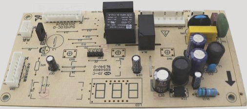
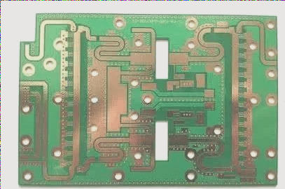
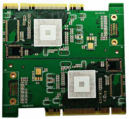
A practical case study demonstrates the importance of effective copper pour design. In a multi-layer PCB, an engineer added a copper ring around the board, as illustrated in Figure 1. Initially, the engineer placed a few vias connecting the copper to the ground plane. However, no vias were added in other areas of the copper region.
Using an **EMSCAN electromagnetic interference scanning system**, the distribution of the electromagnetic field was monitored at a frequency of 22.894 MHz. The results revealed that the PCB with poor grounding—due to insufficient vias connecting the copper pour—generated significant electromagnetic interference (EMI), confirming that proper grounding and via placement are crucial for achieving optimal copper pour performance.
### Conclusion: Weighing the Advantages and Disadvantages
Whether copper pour is an advantageous or disadvantageous technique depends largely on how it is designed and implemented. Properly executed copper pour improves the electrical performance of a PCB, reducing noise and improving signal integrity. However, improper design, such as insufficient via connections or poor grounding, can lead to significant performance degradation and manufacturing challenges.
In conclusion, copper pour remains a powerful tool in PCB design when used with careful attention to detail. Proper grounding, via placement, and copper distribution are essential to fully leverage the benefits of this technique while avoiding potential pitfalls.

In high-frequency applications, the distributed capacitance of the PCB traces plays a significant role in signal integrity. When the trace length exceeds 1/20 of the corresponding wavelength of the noise frequency, an antenna effect can occur, allowing noise to be emitted through the trace. This phenomenon is particularly noticeable in PCBs with interference sources.
For instance, in the case of a 22.894 MHz interference source on the PCB, copper traces or planes can act as both “receiving” and “transmitting” antennas. The PCB copper is sensitive to the interference signal, receiving it as an antenna, and simultaneously emitting strong electromagnetic interference (EMI) externally.
### Frequency-Wavelength Relationship
The relationship between frequency and wavelength is given by the formula:
[
f = frac{C}{lambda}
]
Where:
– ( f ) is the frequency (in Hz)
– ( lambda ) is the wavelength (in meters)
– ( C ) is the speed of light, approximately ( 3 times 10^8 , text{m/s} )
For a signal at 22.894 MHz, the wavelength ( lambda ) is:
[
lambda = frac{3 times 10^8}{22.894 times 10^6} = 13 , text{m}
]
The wavelength divided by 20 ((lambda / 20)) is 65 cm. If the PCB copper traces are longer than this length, the antenna effect can occur. In this case, the trace length exceeds 65 cm, leading to the emission of interference.
### Impact of Rising Edge Frequency
Modern PCBs often use chips with rise times shorter than 1 ns. Assuming a rise time of 1 ns, the resulting electromagnetic interference frequency can be calculated as:
[
f_{text{knee}} = frac{0.5}{T_r} = frac{0.5}{1 , text{ns}} = 500 , text{MHz}
]
For a 500 MHz signal, the wavelength ( lambda ) is:
[
lambda = frac{3 times 10^8}{500 times 10^6} = 0.6 , text{m}
]
Thus, ( lambda / 20 ) is 3 cm. This means that a trace as short as 3 cm on the PCB could act as an antenna for a 500 MHz signal, further exacerbating the EMI problem.
### Best Practices for High-Frequency PCBs
1. **Grounding Considerations**: In high-frequency designs, simply connecting a ground point to the PCB’s ground plane is not sufficient. Proper grounding involves perforating the ground fill near components and ensuring that the ground connections are less than ( lambda / 20 ) in length to achieve effective grounding.
2. **Power Distribution**: When dealing with multiple power sources on a PCB, it is advisable to use power plane splitting technology and employ a single power layer. The power layer, like the ground plane, serves as a reference plane. Effective grounding between the power and ground layers is achieved through the use of multiple filter capacitors. Without adequate filtering, the grounding will be ineffective.
3. **Avoid Copper in Open Areas**: Do not apply copper in open areas of the inner layers of a multilayer PCB unless it can be properly grounded. It is difficult to ensure a “good ground” in these areas, which may contribute to unwanted EMI.
4. **Metal Components**: Metal parts within the equipment, such as heat sinks, metal brackets, and shielding, must be properly grounded to prevent them from acting as unintended antennas and emitting interference.
5. **Regulator Heat Dissipation**: The heat dissipation metal of components like voltage regulators should be adequately grounded. Improper grounding of these components can lead to additional EMI issues.
6. **Crystal Oscillator Grounding**: Ensure that ground isolation strips near crystal oscillators are effectively grounded to prevent noise coupling and reduce the risk of signal interference.
### Conclusion
Proper grounding in PCB design is critical for reducing electromagnetic interference (EMI). By managing the grounding system effectively, you can minimize the signal return path and reduce the impact of external noise emissions. These practices ensure that copper traces on the PCB do not inadvertently act as antennas, and that the overall system operates with optimal signal integrity and minimal EMI. Properly addressing grounding and layout issues can significantly improve the performance of high-frequency circuits and reduce the risk of interference.
Copper pour is a technique in PCB design where unused areas of the board are filled with solid copper, often referred to as copper pour regions. The primary purpose of copper pour is to enhance electrical performance and optimize the physical characteristics of the PCB. However, its effectiveness largely depends on how it’s implemented. Let’s break down the key benefits, challenges, and real-world considerations when using copper pour in PCB design.
### Benefits of Copper Pour in PCB Design
1. **Reduced Ground Impedance**: Copper pour helps to lower the impedance of the ground plane. This can significantly improve the performance of high-speed circuits by providing a low-resistance return path for signals.
2. **Enhanced Noise Immunity**: Copper pours contribute to better shielding and noise reduction. By establishing a continuous ground reference, the copper pour helps to minimize electromagnetic interference (EMI) and improves the board’s overall anti-interference performance.
3. **Improved Power Supply Efficiency**: By reducing the voltage drop across power traces, copper pour can enhance the efficiency of the power distribution network. A more stable and consistent voltage is critical for ensuring the proper operation of sensitive components.
4. **Minimized Loop Area**: Copper pour connected to the ground helps reduce the loop area, which can, in turn, reduce radiated electromagnetic fields and improve the PCB’s overall performance in high-frequency applications.
5. **Prevention of PCB Warping**: During the soldering process, the copper pour helps balance thermal expansion across the board. Filling open areas with copper or grid-like ground traces can reduce the likelihood of PCB warping, ensuring that the board stays flat throughout manufacturing and assembly.
### Challenges and Considerations
While copper pour offers multiple benefits, its implementation must be handled with care. Poorly executed copper pour can lead to a variety of issues, including:
1. **Inadequate Grounding**: In some designs, if copper is connected to the ground plane with too few vias or poor-quality connections, the grounding can be ineffective, leading to increased noise or signal integrity issues.
2. **Imbalance in Copper Distribution**: If copper pour is not evenly distributed or if there are significant unconnected areas, it can create uneven thermal expansion, leading to potential warping or mechanical stress during PCB assembly.
3. **Risk of Short Circuits**: When copper pour is placed too close to sensitive signal traces, there is a risk of unintentional short circuits. Careful clearance must be maintained between copper regions and signal traces to avoid these issues.
4. **Manufacturing Complexity**: While copper pour can reduce manufacturing costs by simplifying trace routing, improper pour configuration can complicate the PCB fabrication process. Special attention is needed to avoid issues such as voids or incomplete copper pours.
### Real-World Example: Impact of Copper Pour on Electromagnetic Field
A practical case study demonstrates the importance of effective copper pour design. In a multi-layer PCB, an engineer added a copper ring around the board, as illustrated in Figure 1. Initially, the engineer placed a few vias connecting the copper to the ground plane. However, no vias were added in other areas of the copper region.
Using an **EMSCAN electromagnetic interference scanning system**, the distribution of the electromagnetic field was monitored at a frequency of 22.894 MHz. The results revealed that the PCB with poor grounding—due to insufficient vias connecting the copper pour—generated significant electromagnetic interference (EMI), confirming that proper grounding and via placement are crucial for achieving optimal copper pour performance.
### Conclusion: Weighing the Advantages and Disadvantages
Whether copper pour is an advantageous or disadvantageous technique depends largely on how it is designed and implemented. Properly executed copper pour improves the electrical performance of a PCB, reducing noise and improving signal integrity. However, improper design, such as insufficient via connections or poor grounding, can lead to significant performance degradation and manufacturing challenges.
In conclusion, copper pour remains a powerful tool in PCB design when used with careful attention to detail. Proper grounding, via placement, and copper distribution are essential to fully leverage the benefits of this technique while avoiding potential pitfalls.
In high-frequency applications, the distributed capacitance of the PCB traces plays a significant role in signal integrity. When the trace length exceeds 1/20 of the corresponding wavelength of the noise frequency, an antenna effect can occur, allowing noise to be emitted through the trace. This phenomenon is particularly noticeable in PCBs with interference sources.
For instance, in the case of a 22.894 MHz interference source on the PCB, copper traces or planes can act as both “receiving” and “transmitting” antennas. The PCB copper is sensitive to the interference signal, receiving it as an antenna, and simultaneously emitting strong electromagnetic interference (EMI) externally.
### Frequency-Wavelength Relationship
The relationship between frequency and wavelength is given by the formula:
[
f = frac{C}{lambda}
]
Where:
– ( f ) is the frequency (in Hz)
– ( lambda ) is the wavelength (in meters)
– ( C ) is the speed of light, approximately ( 3 times 10^8 , text{m/s} )
For a signal at 22.894 MHz, the wavelength ( lambda ) is:
[
lambda = frac{3 times 10^8}{22.894 times 10^6} = 13 , text{m}
]
The wavelength divided by 20 ((lambda / 20)) is 65 cm. If the PCB copper traces are longer than this length, the antenna effect can occur. In this case, the trace length exceeds 65 cm, leading to the emission of interference.
### Impact of Rising Edge Frequency
Modern PCBs often use chips with rise times shorter than 1 ns. Assuming a rise time of 1 ns, the resulting electromagnetic interference frequency can be calculated as:
[
f_{text{knee}} = frac{0.5}{T_r} = frac{0.5}{1 , text{ns}} = 500 , text{MHz}
]
For a 500 MHz signal, the wavelength ( lambda ) is:
[
lambda = frac{3 times 10^8}{500 times 10^6} = 0.6 , text{m}
]
Thus, ( lambda / 20 ) is 3 cm. This means that a trace as short as 3 cm on the PCB could act as an antenna for a 500 MHz signal, further exacerbating the EMI problem.
### Best Practices for High-Frequency PCBs
1. **Grounding Considerations**: In high-frequency designs, simply connecting a ground point to the PCB’s ground plane is not sufficient. Proper grounding involves perforating the ground fill near components and ensuring that the ground connections are less than ( lambda / 20 ) in length to achieve effective grounding.
2. **Power Distribution**: When dealing with multiple power sources on a PCB, it is advisable to use power plane splitting technology and employ a single power layer. The power layer, like the ground plane, serves as a reference plane. Effective grounding between the power and ground layers is achieved through the use of multiple filter capacitors. Without adequate filtering, the grounding will be ineffective.
3. **Avoid Copper in Open Areas**: Do not apply copper in open areas of the inner layers of a multilayer PCB unless it can be properly grounded. It is difficult to ensure a “good ground” in these areas, which may contribute to unwanted EMI.
4. **Metal Components**: Metal parts within the equipment, such as heat sinks, metal brackets, and shielding, must be properly grounded to prevent them from acting as unintended antennas and emitting interference.
5. **Regulator Heat Dissipation**: The heat dissipation metal of components like voltage regulators should be adequately grounded. Improper grounding of these components can lead to additional EMI issues.
6. **Crystal Oscillator Grounding**: Ensure that ground isolation strips near crystal oscillators are effectively grounded to prevent noise coupling and reduce the risk of signal interference.
### Conclusion
Proper grounding in PCB design is critical for reducing electromagnetic interference (EMI). By managing the grounding system effectively, you can minimize the signal return path and reduce the impact of external noise emissions. These practices ensure that copper traces on the PCB do not inadvertently act as antennas, and that the overall system operates with optimal signal integrity and minimal EMI. Properly addressing grounding and layout issues can significantly improve the performance of high-frequency circuits and reduce the risk of interference.