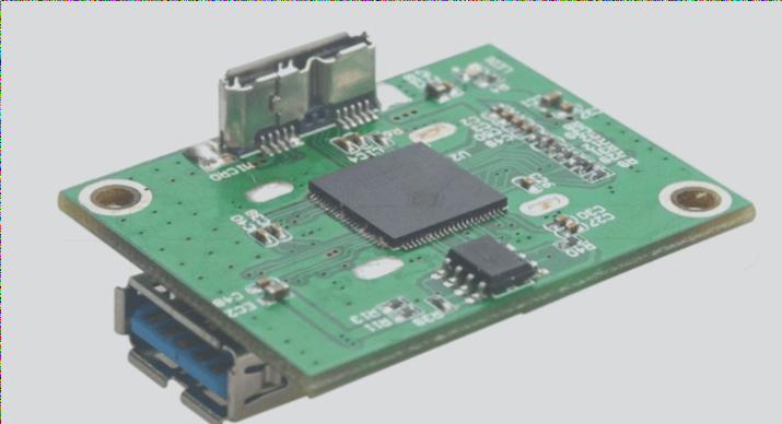
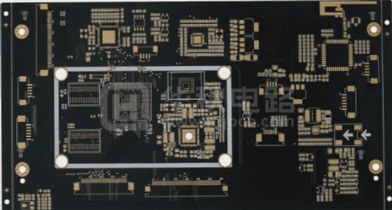
The Importance of Copper Layering in PCB Circuit Boards
Enhancing Performance and Functionality
- Heat Dissipation: Copper layers are vital for efficient heat dissipation, ensuring the reliable operation of PCB components by preventing overheating.
- Shielding and Anti-Interference: Copper acts as a shield against electromagnetic interference, maintaining signal integrity and reducing noise.
- Structural Strength: Copper enhances the mechanical strength of PCBs, reducing the risk of damage during handling and operation.
- Aesthetic Appeal: Copper-clad boards offer a sleek and polished appearance, ideal for consumer electronics and industrial applications.
- Counterfeit Protection: Copper layers with specialized treatments add complexity, making it harder for counterfeiters to replicate PCB designs.
PROTEL’s Innovative Copper Layering Approach
- Area Identification: Define areas requiring copper coating based on design specifications.
- Copper Network Selection: Choose the type of copper network for optimal performance.
- Precision Tools: Utilize PROTEL’s copper layering tool for accurate placement and configuration.
- Safety Parameters: Set spacing, line widths, and grid parameters to prevent electrical issues.
- Layering Methods: Select between positive or oblique grid methods based on design goals.
Optimizing Copper Layering Settings
Adjusting copper settings is crucial to ensure PCB performance aligns with design requirements, covering aspects like heat dissipation and interference prevention.

Net Option Group: Copper Network Settings
The Net Option group manages copper connections on the PCB, offering settings for network connection, copper coverage, and removal of isolated copper regions.
Hatching Style: Copper Pouring Method
The Importance of Hatching Style in PCB Design
- The hatching style in PCB design determines the pattern for copper filling, offering options like 90° (Vertical), 45° (Diagonal), Vertical, and Horizontal.
- Choosing the right hatching style is crucial for high-frequency applications as it impacts electrical performance.
- The style influences the direction and arrangement of copper traces, affecting thermal conductivity and resistance.
Plane Settings: Copper Grid and Line Properties
- Grid Size specifies the spacing between copper areas, affecting overall copper density.
- Trace Width determines the width of copper traces, crucial for electrical performance.
- Layer defines where copper will be placed, essential for multi-layer PCBs.
- Lock Primitives option prevents accidental edits and should be selected after finalizing the copper layout.
Surround Pads With: Copper Pad Encapsulation
- Two main wrapping styles for pads: 8-Sided Encapsulation and Arc Encapsulation.
- Choosing the appropriate style is essential for solder joint integrity and preventing shorts.
Minimum Primitives Size: Copper Trace Minimum Length
- Setting the minimum length for copper traces affects pouring speed and design flexibility.
- Track Width and Grid Size should meet minimum requirements to avoid errors during copper pouring.
Handling Dead Copper and Layer Optimization
- Avoid immediate removal of dead copper to prevent large empty regions on the board.
- Connect isolated regions using vias or multi-layer copper connections to optimize the layout.
For more efficient modifications in Protel99, consider deleting and reapplying copper paving to ensure precision in PCB design adjustments.
The Importance of Copper Layout in PCB Design
Creating a proper copper layout is essential for maximizing the electrical and thermal performance of a printed circuit board (PCB). By delving into key settings such as the Net Option group, Hatching Style, Plane Settings, and Minimum Primitives Size, designers can enhance the copper pour process, leading to improved connectivity and higher overall PCB quality.
- Optimizing Copper Pour Process
- Enhancing Connectivity
- Improving PCB Quality
Moreover, strategies like eliminating excess copper, refining layer connections, and leveraging Protel99’s copper editing tools can significantly enhance the reliability and manufacturability of the final PCB product.