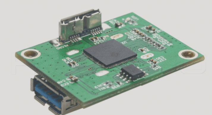
1. In the PCB design of typical products, the layout of components is usually established first, followed by the routing of connections. The interference issues are primarily addressed at the component placement stage, after which the details of the wiring are refined.

2. With the current design trends in mobile phones and tablets, product sizes have been consistently reduced and made thinner, while the number of additional features has not diminished; in fact, it has increased. Even the operating clock speed of core processor components continues to rise. Today’s mobile devices often feature processors with clock frequencies ranging from 1 to 1.5 GHz. If the numerous high-frequency components in these devices are not carefully managed during the circuit board layout, suboptimal designs could adversely affect the performance of multimedia applications, including video and audio.

3. Taking mobile phones and smartphones as examples, the available space for internal mechanical design can be described as extremely limited. This constraint applies not only to components but also to subsystems such as batteries, display panels, backlight modules, camera modules, and logic circuit boards…


1. The extremely stacked and high-density configurations, combined with the performance and functionality demands of modern products, complicate the design of mobile devices. Developers must address not only the actual connections among various components and subsystems but also potential interference between these systems.

2. The signal quality in the audio circuit is crucial for the overall user experience, making careful circuit layout essential.

3. The PCB space available in mobile phones is limited, and adopting a one-chip design offers a cost-effective solution. Differentiating between various subsystems and minimizing noise interference is key to effective design.

4. Particularly in printed circuit board layout design, this becomes one of the most significant challenges in mobile phone development. The different subsystems may have conflicting design requirements. For instance, the wireless module demands optimal antenna performance and superior wireless transmission, while the digital logic computing core necessitates a stable computing environment. Integrating these two systems into a compact device requires optimizing wireless radio frequency transmission while ensuring digital logic circuits operate stably in an environment that isolates external noise. The challenge lies in creating a single carrier board that accommodates both systems without interference.

5. A well-designed PCB must provide optimized operating conditions and environments for each component, functional block, or module while minimizing mutual interference among various subsystems. In practice, the conflicting design requirements of different subsystems often necessitate engineering compromises or the implementation of reinforcement measures, such as adding metal barriers. However, such measures can lead to an increase in PCB size, conflicting with the design goals of light, thin, and short products.

6. Addressing radio frequency signal interference is relatively straightforward when dealing with digital logic circuits, as the digital subsystem operates in binary (0 or 1) and can overlook minor radio frequency disruptions. Conversely, for multimedia applications (like video playback or MP3 music), radio frequency interference can significantly degrade the user experience.

7. During the standard development process, the initial step before designing the PCB is arranging component layouts. At this stage, it’s essential to consider optimal wiring benefits (shortest distances for PCB space efficiency), while also establishing a ground plane to minimize potential noise issues.

8. In terms of component layout, functional subsystems can usually be divided into distinct blocks. RF components that may cause interference should be positioned as close to the device’s antenna as possible, typically at the board’s corners, while RF functions can be shielded with metal. The core digital logic system, which also operates at high frequencies, is generally located at the center of the PCB. This positioning not only aids in heat dissipation from the processor but also supports effective functional layout. The audio circuit, which most impacts user perception, is a critical focus during carrier board development, necessitating accumulated design experience to optimize wiring layout and minimize interference.

9. In a hybrid system circuit that merges communication, networking, and digital operations like those in mobile phones, effectively separating analog and digital circuits is essential to prevent interference. Commonly, different circuits are divided across multiple carrier boards, with key connections made via cables to facilitate effective functional system separation.

10. However, due to cost constraints, the current trend in multi-carrier design emphasizes minimizing the size of the carrier board for maximum functional integration, leading to challenges in separating digital and analog circuits. The design approach can segment the overall carrier board into digital and analog blocks, achieving a separation effect similar to distinct carrier boards. Additionally, while radio frequency circuits are also considered analog, they differ from audio processing. Radio frequency signals can couple and interfere with audio circuits, creating unwanted noise. Thus, maximizing the distance between the radio frequency, wireless network, and audio circuit subsystems is beneficial for reducing audio interference.

11. The design complexity of analog circuits can surpass that of digital circuits, necessitating more extensive design experience for functional enhancement. For example, positioning the audio amplifier chip closer to the audio connector minimizes PCB circuit losses and results in purer sound output. Most mobile devices utilize high-performance Class D audio amplifier circuits, which must also account for electromagnetic interference (EMI) during design.

12. After segmenting the PCB into analog, digital, and radio frequency zones, the arrangement of components in the analog section should prioritize the shortest audio signal path. The audio amplifier must be positioned as close as possible to the headphone jack and speaker to effectively reduce EMI from the Class D speaker amplifier, while also addressing the suppression of additional noise from headphone signals. This will ensure that the audio transmission circuit distance is minimized, ultimately enhancing the product’s audio performance.


Let me know if you need any further adjustments!

Leave a Comment

Contact

WellCircuits
More than PCB

Upload your GerberFile(7z,rar,zip)