1. The forward design of integrated circuits in PCB design
The integrated circuit design occurs once the user has clearly defined the circuit principles, functions, various parameter metrics, and economic considerations.
The specific process is as follows:
Reverse design of integrated circuits
Reverse design entails fully replicating an existing integrated circuit chip, making partial modifications to the original chip, or reducing the chip’s area to cut costs.
The specific process:
Design and optimization of household system schemes.

1. We currently offer comprehensive system solutions that span high-end products such as GPS, MP3 players, and tax control machines, to mid-range consumer electronics like digital radios, home appliance control panels, CNC machine tools, and other industrial control products, down to low-end toy electronics. Additionally, we can integrate our solutions into existing systems for users, helping to reduce costs and enhance product competitiveness in the market.
2. Anatomical Analysis of Integrated Circuits and Photomicrographs
We can conduct anatomical analyses and microphotography of various packaged integrated circuits, achieving magnifications of up to 4000 times. The specific process is as follows:
3. Memory Code Point Extraction
As integrated circuits continue to evolve, chip sizes are expanding. Most chips incorporate storage devices like ROM to retain user data or programs. Extracting code points from ROM is crucial for system design or reverse engineering of chips. ROM code points typically exist in two formats: plain code and mask-type code. For plain code, we utilize our proprietary software for direct extraction. For mask-type code points, dyeing must occur before extraction. (We have successfully extracted over 32M MASK ROM).
4. Imitation Design of Surface Acoustic Wave Devices (SAW) and High-Power Tubes
We employ graphic tools to design surface acoustic wave devices (SAW) and high-power tubes. For SAW devices, we can replicate models below 2GHz, maintaining geometric errors within two thousandths. Additionally, we can produce and package SAW devices operating under 800MHz. The layout of high-power tubes is typically unique, featuring many irregular shapes that can be accurately created by merging graphic tools with specialized processing programs.
5. Pads on SMT-PCB
1) For SMT components on the wave soldering surface, the pads of larger components (like transistors and sockets) should be slightly enlarged. For instance, SOT23 pads can be extended by 0.8-1mm to avoid shadowing effects caused by components.
2) PCB pad sizes should correspond to the component dimensions. The pad width should match or slightly exceed the width of the component’s electrode for optimal soldering results.
3) Between two connected components, avoid a single large pad, as solder can bridge the components, leading to undesired connections. Instead, connect the pads of the two components separately with a thinner wire. If higher currents are needed, multiple wires can be run in parallel, covered with green oil.
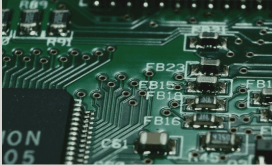
4) Avoid through holes on or near SMT component pads, as solder may flow through these holes during the reflow process, leading to cold solder joints or shorts on the opposite side of the PCB.
The integrated circuit design occurs once the user has clearly defined the circuit principles, functions, various parameter metrics, and economic considerations.
The specific process is as follows:
Reverse design of integrated circuits
Reverse design entails fully replicating an existing integrated circuit chip, making partial modifications to the original chip, or reducing the chip’s area to cut costs.
The specific process:
Design and optimization of household system schemes.
1. We currently offer comprehensive system solutions that span high-end products such as GPS, MP3 players, and tax control machines, to mid-range consumer electronics like digital radios, home appliance control panels, CNC machine tools, and other industrial control products, down to low-end toy electronics. Additionally, we can integrate our solutions into existing systems for users, helping to reduce costs and enhance product competitiveness in the market.
2. Anatomical Analysis of Integrated Circuits and Photomicrographs
We can conduct anatomical analyses and microphotography of various packaged integrated circuits, achieving magnifications of up to 4000 times. The specific process is as follows:
3. Memory Code Point Extraction
As integrated circuits continue to evolve, chip sizes are expanding. Most chips incorporate storage devices like ROM to retain user data or programs. Extracting code points from ROM is crucial for system design or reverse engineering of chips. ROM code points typically exist in two formats: plain code and mask-type code. For plain code, we utilize our proprietary software for direct extraction. For mask-type code points, dyeing must occur before extraction. (We have successfully extracted over 32M MASK ROM).
4. Imitation Design of Surface Acoustic Wave Devices (SAW) and High-Power Tubes
We employ graphic tools to design surface acoustic wave devices (SAW) and high-power tubes. For SAW devices, we can replicate models below 2GHz, maintaining geometric errors within two thousandths. Additionally, we can produce and package SAW devices operating under 800MHz. The layout of high-power tubes is typically unique, featuring many irregular shapes that can be accurately created by merging graphic tools with specialized processing programs.
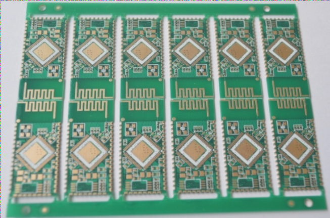
5. Pads on SMT-PCB
1) For SMT components on the wave soldering surface, the pads of larger components (like transistors and sockets) should be slightly enlarged. For instance, SOT23 pads can be extended by 0.8-1mm to avoid shadowing effects caused by components.
2) PCB pad sizes should correspond to the component dimensions. The pad width should match or slightly exceed the width of the component’s electrode for optimal soldering results.
3) Between two connected components, avoid a single large pad, as solder can bridge the components, leading to undesired connections. Instead, connect the pads of the two components separately with a thinner wire. If higher currents are needed, multiple wires can be run in parallel, covered with green oil.
4) Avoid through holes on or near SMT component pads, as solder may flow through these holes during the reflow process, leading to cold solder joints or shorts on the opposite side of the PCB.

