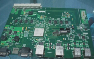
Guidelines for Effective PCB Layout
When designing a printed circuit board (PCB), it is crucial to consider the positioning of components and the placement of decoupling capacitors to enhance interference resistance and circuit reliability. Here are some key points to keep in mind:
Component Arrangement:
- Position interrelated components, such as the clock generator, crystal oscillator, and CPU clock input, close to each other to minimize noise susceptibility.
- Keep noise-prone devices away from logic control and storage circuits of the microcontroller.
- Consider designing circuits as separate PCBs for better interference resistance.
Decoupling Capacitors:
- Install decoupling capacitors near key components like ROM and RAM to reduce inductance effects and noise spikes.
- Use 0.1uF ceramic capacitors for effective noise mitigation on the Vcc trace.
- Avoid tantalum capacitors for higher impedance at elevated frequencies.
Placement Tips for Decoupling Capacitors:
- Connect a 100µF electrolytic capacitor across the power input, opting for larger capacitance if space permits.
- Position a 0.01µF ceramic capacitor close to each integrated circuit chip.
- Connect decoupling capacitors for components with weak interference resistance and significant current changes.
- Keep capacitor leads short, especially for high-frequency bypass capacitors.
Ground Layout:
- Separate logic ground and analog ground, connecting them to appropriate power ground lines.
- Design a closed loop ground wire for logic circuits to improve interference resistance.
- Use thick ground wires to minimize resistance and potential shifts.
- Select grounding points carefully to minimize interference.
- Maximize trace width based on current size and align power and ground line routing with data lines.
- Utilize wide data line widths to reduce impedance and cover the PCB bottom layer with ground wires for improved interference resistance.
Data Line Considerations:
- Ensure data line width is at least 0.3 mm (12 mil) and ideally 0.46 to 0.5 mm (18 mil to 20 mil) to minimize impedance.

Latest Updates in PCB Technology
1. Introduction to PCBs
Printed Circuit Boards (PCBs) are essential components in electronic devices, providing a platform for connecting and supporting various electronic components.
2. Advancements in PCB Design
Recent developments in PCB design include the use of flexible and rigid-flex PCBs, high-speed digital signaling, and miniaturization of components.
3. Emerging Trends in PCB Manufacturing
Industry trends such as additive manufacturing, Internet of Things (IoT) integration, and environmental sustainability are shaping the future of PCB manufacturing.
4. Importance of Quality Control in PCB Production
Ensuring quality control measures in PCB production is crucial for reliability, performance, and compliance with industry standards.
5. Future Prospects of PCB Technology
The future of PCB technology looks promising with advancements in materials, design software, and automation, leading to more efficient and reliable electronic devices.