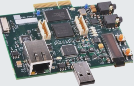
When the PCB design is completed, it is essential to perform functional inspections on all elements. Just like when we review our own examination papers, we need to conduct a thorough analysis and recheck all the questions to avoid major mistakes due to oversight. The same principle applies to PCB design. The following inspection items need to be carried out after PCB design:
1. DFM review of the PCB: Ensure that the PCB design meets the manufacturing process requirements, including trace width, spacing, routing, layout, vias, markings, and component orientation for wave soldering.
2. Verify component and pad alignment: Check if the actual SMT components match the designed pads (indicate any discrepancies with a red mark) and ensure they comply with the minimum spacing requirements for the placement machine.
3. Generate three-dimensional models: Create three-dimensional models to verify that components do not interfere with each other, evaluate whether the component layout is reasonable, assess heat dissipation effectiveness, and confirm that the design supports optimal heat absorption during SMT reflow soldering.
4. Optimization of PCBA Production Line: Optimize the placement sequence and material station locations. Input the details of existing placement machines (e.g., Siemens high-speed machines, global multifunction machines) into the software, and allocate components on the board. Determine the types and locations of Siemens pastes and other global components, including their locations and pickup points. This will help optimize the SMT patch processing program and save time. For multi-line production, component placement can also be optimized.
5. Work Instructions: Automatically generate work instructions for workers on the production line.
6. Revision of Inspection Rules: Modify inspection rules as needed. For instance, adjust the minimum component spacing from 0.1mm to 0.2mm based on the specific model, manufacturer, and board complexity. Similarly, change the minimum wire width from 6mil to 5mil for high-density designs.
7. Support for Placement Software: Support Panasonic, Fuji, and Universal placement software. This will allow for automatic generation of placement programs, reducing programming time.
8. Automatically Generate Steel Plate Optimization Graphics.
9. Automatically Generate AOI and X-RAY Programs.
10. Inspection Report.
11. Support Various Software Formats: Include formats from Japan, US KATENCE, and China PROTEL.
12. Review the BOM: Correct any errors, such as spelling mistakes by the manufacturer, and convert the BOM table into the appropriate software format.
The Manufacturing Process of Double-Sided PCBs:
The manufacturing process for double-sided PCBs involves several steps. Start with blanking the double-sided copper-clad laminate, followed by composite board CNC drilling. Next, perform through-hole inspection, deburring, brushing, and chemical plating for through-hole metallization. Proceed with full-board electroplating, thin copper inspection, and cleaning. Screen print the negative circuit pattern, then cure with dry or wet film, exposure, and development. Inspect and repair the circuit pattern, then apply electroplated tin, anticorrosive nickel, or gold. Remove printing materials and etch copper. Finally, remove tin and clean, apply a layer of thermal curing green oil, screen print the solder mask pattern, and cure with either photosensitive dry film or wet film. Clean, dry, and apply screen printing for mark character graphics. Finally, spray tin or apply an organic solder mask, shape, clean, dry, test electrically, inspect packaging, and deliver the finished product.
As product requirements increase, ordinary single-layer PCBs are no longer sufficient. This has led to the development of double-sided printed circuit boards (PCBs), which feature conductive lines on both sides of the board. Typically made from epoxy glass cloth copper-clad laminate, these boards are used in communication electronic equipment, advanced instruments, high-performance computers, and more. The typical process for manufacturing double-sided plated-hole printed boards is the bare copper-clad solder mask process (SMOBC), which includes the following steps:
1. Blanking double-sided copper-clad laminate
2. Composite board CNC drilling
3. Through-hole inspection, deburring, and brushing
4. Electroless plating (through-hole metallization)
5. Full-board electroplating of thin copper
6. Inspection and cleaning
7. Screen printing negative circuit patterns
8. Curing with dry or wet film, exposure, and development
9. Circuit pattern inspection and repair
10. Electroplating tin, anticorrosive nickel, or gold
11. Removal of photosensitive film and printing material
12. Etching copper and removing tin
13. Cleaning and applying thermal curing green oil
14. Screen printing solder mask pattern and curing
15. Cleaning, drying, screen printing mark character graphics
16. Curing, spray tin or applying organic solder mask
17. Shaping, cleaning, drying, electrical switch testing, packaging inspection, and finished product delivery.
More complex multi-layer PCBs may involve additional processes. These steps encompass PCB manufacturing, component procurement, SMT patching, assembly, and testing.