The Importance of PCB Board Design for Radio Frequency Switch Modules
The design of the PCB board for the functional circuit of the radio frequency switch module is crucial in advancing modern wireless communication systems, including mobile communication, radar, satellite communication, and related technologies. These systems have strict requirements for switching speed, power capacity, and transceiver switch integration.
One of the latest developments in this field is the research and development of bus technology, especially for military-grade bus modules, which play a significant role in meeting the demands of these advanced communication systems.
Implementing Virtual Instrumentation in Hardware Circuits
The concept of virtual instrumentation is employed to implement hardware circuits in software. This allows the radio frequency switch module to be directly controlled by a computer and seamlessly integrated into the bus test system. The application of computer and microelectronics technology in testing fields presents promising avenues for development.

Design and Implementation of VXI Bus Interface Circuit
The VXIbus is an extension of VMEbus in the field of instrumentation, offering a modular automatic instrument system operated by a computer. It emphasizes standardization and modularity to achieve serialization, generalization, and interchangeability of instruments. The VXI bus’s open architecture and PlugPlay mode meet the requirements of information products, providing high-speed data transmission, compact structure, flexible configuration, and good electromagnetic compatibility.
- VXI Bus Devices Categorization: register-based, message-based, and memory-based
- Advantages of VXI Bus: high-speed data transmission, compact structure, flexible configuration
- Components of VXI Bus Register Base Interface Circuit: bus buffer drive, addressing and decoding circuit, data transmission response state machine, configuration and operation register group
Bus Buffer Driver
The bus buffer driver manages data, address, and control line buffering in the VXI backplane bus to comply with VXI specification signals. It utilizes two 74LS245 chips strobed by DBEN* generated by the data transmission response state machine.
Addressing and Decoding Circuit
This circuit decodes addressing lines A01 to A31, data strobe lines DS0* and DS1*, and control lines, designed using MAX+PLUS2 schematic design with components like 74688 and 74138. It compares received address information with the logical address set by the hardware address switch for device addressing.
Data Transmission Response State Machine
Designed using MAX+PLUS2, this module configures VXI backplane bus control signals for standard data transmission cycles, providing essential timing and control signals for data transmission completion.
VXI Bus Device Configuration Registers
- Integration of configuration registers in VXI bus devices allows the main controller to access crucial device information.
- Registers include identification, device type, status, and control registers.
- Design utilizes MAX+PLUS2 schematic design with 74541 chip and associated modules.
- ID, DT, and ST registers are read-only, while control registers are write-only.
- VXI bus primarily controls switches for switch state control and status queries.
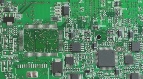
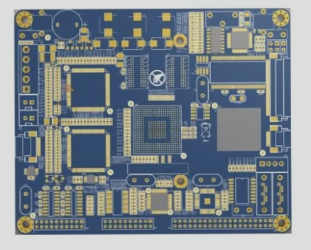
Module Function Circuit Board Design
- VXI bus devices enable retrieval of fundamental device details.
- RF circuit board operates within a frequency range of 10kHz to 300GHz.
- Special attention required for RF signal effects in circuit board design.
- RF switch circuit controlled by VXI bus to mitigate interference.
Component Layout
- Electromagnetic compatibility (EMC) crucial for electronic system functionality.
- RF circuit PCB design focuses on minimizing radiation and anti-interference capabilities.
- Component layout impacts circuit interference and performance.
Wiring
- Low-density designs preferred for signal impedance matching.
- RF circuits require careful signal line direction, width, and spacing considerations.
- Comprehensive RF circuit PCB design needed for effective wiring.
Power and Grounding
- Correct power and ground wiring essential for RF circuit PCB design.
- Short, thick power lines and consistent alignment with data transmission direction recommended.
- Four-layer PCB design isolates RF signal lines for optimal performance.
Conclusion
VXI bus system serves as a global modular instrument bus system, accommodating various vendors and setting the standard for instrument buses. This article focuses on the development of a VXI bus-based radio frequency switch module, emphasizing user-friendly operation.


 العربية
 简体中文
简体中文 Nederlands
 English
 Français
 Deutsch
 Italiano
 日本語
日本語 한국어
한국어 Português
 Русский
 Español
 ไทย
ไทย