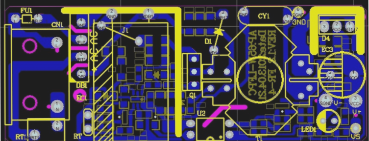
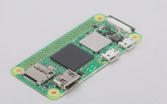
2. Among the PCB substrates currently available on the market, FR4 is the most commonly used. FR4 is a glass fiber reinforced epoxy resin laminate, and the PCB can be single-layer or multi-layer.
3. When the size of the touch module is limited, it is not always feasible to use a single-layer PCB; typically, a four-layer or two-layer PCB is employed. Let’s take the commonly used two-layer PCB as an example to introduce PCB layout guidelines.
4. PCB Design and Layout
5. In a two-layer PCB, the S-TouchTM touch controller and other components are placed on the bottom layer of the PCB, while the sensor electrodes are placed on the top layer of the PCB.

Level 1 (top layer)
1. The sensor electrode is located on the top layer of the PCB (the upper end of the PCB is fixed with the overlay board). To enhance sensitivity, it is recommended to use a sensing electrode with dimensions of 10 x 10 mm. Although a smaller sensing electrode can be used, it will result in reduced sensitivity. Additionally, it is advisable that the size of the sensing electrode does not exceed 15 x 15 mm. Exceeding this size can not only decrease sensitivity but also increase susceptibility to noise.
2. The blank area can be filled with grounded copper foil (with a trace width of 6 mils and a grid size of 30 mils).
3. The top layer can be utilized for laying common signal traces (excluding sensor signal traces). Sensor signal traces should be routed on the bottom layer whenever possible.
4. The distance between the sensing electrode and the grounded copper foil should be at least 0.75 mm. No plug-ins, no viruses.
Layer 2 (bottom layer)
1. The S-Touch™ controller and other passive components should be placed on the bottom of the PCB.
2. Sensor signal traces will be routed on the bottom layer. Ensure that the sensor signal traces of one channel do not run beneath the sensing electrodes of other channels.
Sensor signal trace routing method under the touch plate
1. The blank area can be filled with grounded copper foil (with a trace width of 6 mils and a grid size of 30 mils).
2. The distance between the sensor signal trace and the grounded copper foil should be at least twice the width of the sensor signal trace.
3. To minimize crosstalk, maximize the distance between two sensing electrodes or sensing signal traces. Where feasible, place grounded copper foil between these sensing electrodes or signal traces.
4. The length of the sensor signal trace does not need to be exactly the same across channels. With the use of matching tuning capacitors, the input capacitance between channels can be balanced. However, if PCB space permits, it is preferable to use sensor signal traces of equal length (and uniform electrode sizes). This allows for a single standard reference capacitor to adjust all sensing channels’ capacitive reactance within the controller’s dynamic range, thereby simplifying PCB design.
5. Clock, data, or periodic signal traces should not be routed parallel to or adjacent to the sensor signal traces. These signal lines should be as perpendicular as possible to the sensor signal traces or routed in different areas of the PCB. No plug-ins, no viruses.
6. If clock, data, or periodic signal traces must run parallel to sensor signal traces, they should be on different layers and not overlap. Minimize the length of the parallel segments of the signal traces as much as possible.
In the previous discussion of the two-layer FR4 PCB, grounded copper foil was used to fill the blank areas of the PCB. The grounded copper foil helps shield the touch module from external noise and stabilizes the inherent capacitance of the sensor circuit.
However, there are several issues to consider when using grounded copper foil. It increases the inherent capacitance of the sensor and also raises the potential for false detection due to water droplets.


