Designing a Switching Power Supply Layout: Best Practices
- Place the transformer.
- Design the PCB power switch current loop.
- Design the output rectifier current loop.
- Connect the control circuit to the AC power circuit.
- Design the input current source loop and input filter.
When designing the output load loop and output filter, it is essential to follow these principles:
- Consider the PCB size: Opt for a rectangular shape with aspect ratios of 3:2 or 4:3 to balance trace lengths and heat dissipation.
- Place components for easy soldering and avoid overly dense placements.
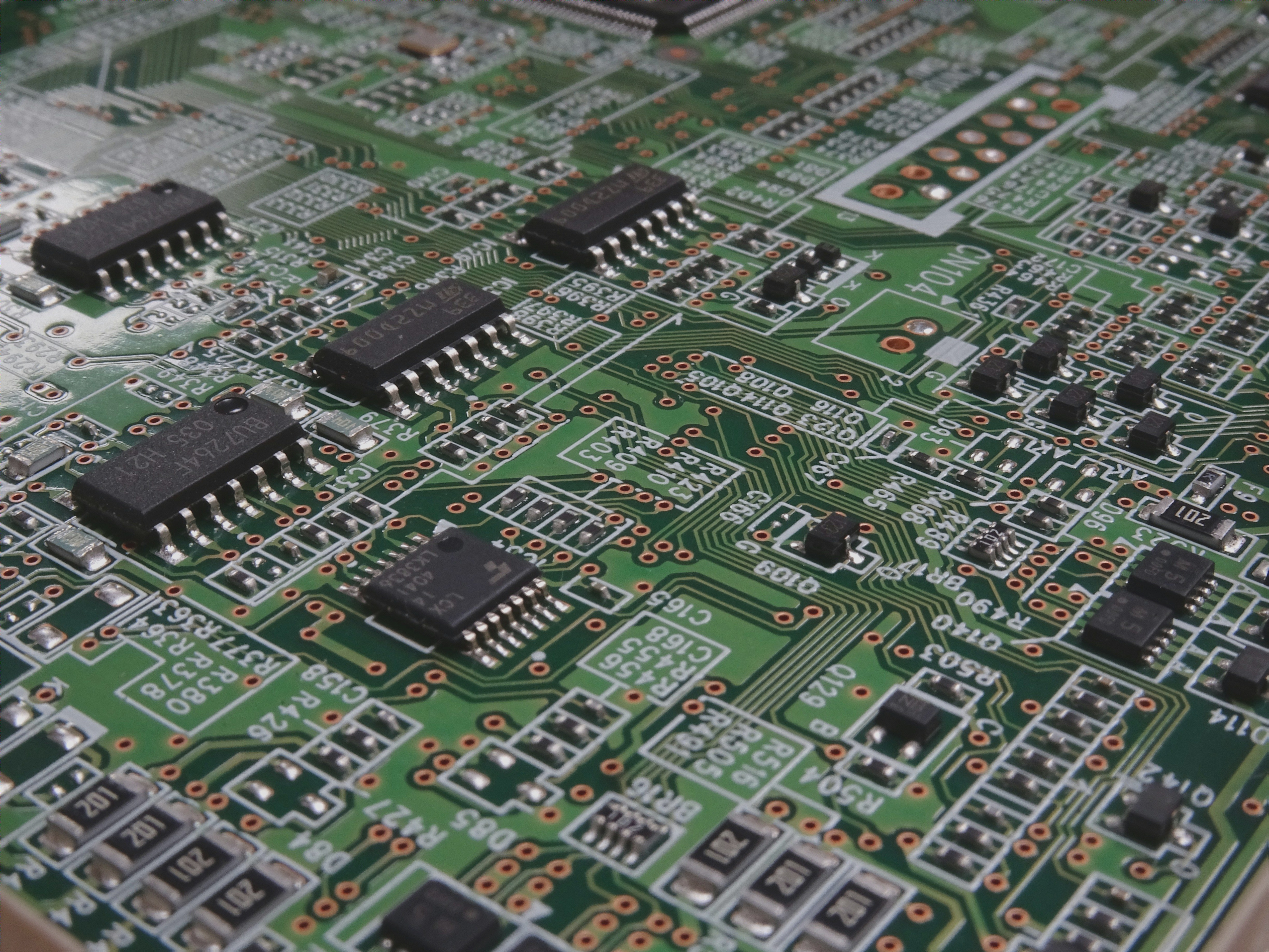
- Position core components centrally and arrange surrounding components neatly.
- For high-frequency circuits, parallel component arrangement simplifies installation and mass production.
- Arrange functional circuit units based on signal flow for efficient circulation.
- Maximize routing efficiency to reduce radiation interference.
Wiring Considerations
High-frequency signals in a switching power supply can impact trace impedance and inductance. To minimize interference:
- Keep traces carrying AC current short and wide to reduce impedance.
- Adjust trace length and width to control frequency response and RF energy radiation.
- Align power and ground traces to improve noise immunity and reduce loop resistance.
- Grounding is crucial for controlling interference; carefully plan ground trace placement.
Design Verification
Important Considerations for PCB Design Verification
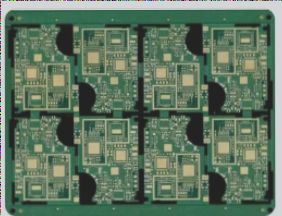
In 2018, Shenzhen Jiali announced a significant price reduction for bulk PCB orders, making it an attractive option for businesses. Once the routing design is completed, thorough verification is crucial to ensure the layout meets the designer’s specifications and aligns with the production process rules.
Key Elements to Review in PCB Design
- Design rules
- Layer definitions
- Trace widths and spacing
- Pad designs and via configurations
- Component placement
- Power and ground network layout
- High-speed signal routing
- Clock network shielding
- Decoupling capacitor placement
Design Output Precautions
When exporting Gerber files, it is essential to include routing layers, silk screen layers, solder mask layers, and drilling layers. Pay attention to the silk screen layer configuration to ensure the correct elements are selected. Make sure to include the board outline for each layer and use PowerPCB for generating drilling files.
If you require PCB manufacturing services, feel free to contact us.