Wafer Level Packaging (WLCSP) for High-Performance PCB Integration
Wafer level packaging (WLCSP) is an advanced chip-scale package (CSP) technology that facilitates the mounting of integrated circuits (ICs) face down onto printed circuit boards (PCBs). This innovative approach involves connecting the chip’s solder joints to the PCB pads using individual solder balls, eliminating the need for additional filling materials.
Key Advantages of WLCSP Technology
- Minimized inductance between the IC and the PCB, crucial for high-speed applications
- Reduced package size, production cycle time, and enhanced thermal conductivity
Maxim’s UCSP Technology
Maxim’s WLCSP technology, known as Ultra Chip Scale Package (UCSP), offers a surface that provides electrical isolation. The UCSP package utilizes a photolithographic process to create vias in the BCB (benzocyclobutene) film for electrical connections to the IC’s substrate. An Under Ball Metal (UBM) layer is applied to these vias to enhance the electrical interface.
UCSP Solder Ball Array
A cross-sectional view of a typical UCSP structure reveals a rectangular grid arrangement of the solder ball array with a uniform pitch between the balls. The array usually consists of 2 to 6 rows and columns.

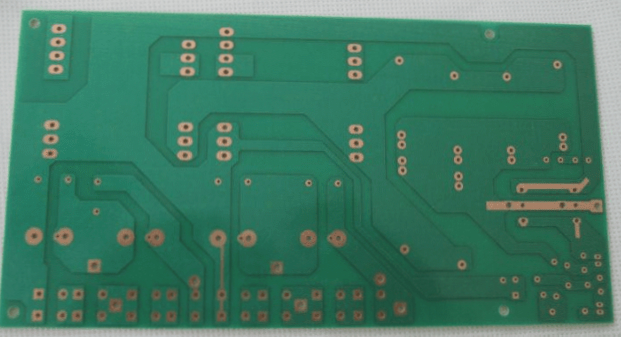
Design Principles and PCB Manufacturing for UCSP Integration
Successful integration of UCSP components requires careful attention to the PCB layout. The design principles and manufacturing specifications for the UCSP pad structure differ from traditional lead-type devices and laminate-based BGA components.
Solder Mask Defined (SMD) vs. Non-Solder Mask Defined (NSMD) Pads
When designing PCBs for UCSP integration, choosing between SMD and NSMD pads is crucial. Considerations such as power, ground, and signal routing play a significant role in determining the appropriate pad type. It is essential to maintain symmetry in the layout of UCSP pads and traces to ensure proper solder joint wetting and prevent off-center connections.
Advantages of NSMD Pads:
- Enhanced control in copper trace etching process
- Improved flexibility for trace routing
- Increased assembly tolerance
Advantages of SMD Pads:
- Allow for wider copper traces, reducing inductance
- Can enhance electrical performance
For your PCB manufacturing needs or inquiries, feel free to contact us.